cmut fabrication based on a thick buried oxide layer - Khuri-Yakub ...
cmut fabrication based on a thick buried oxide layer - Khuri-Yakub ...
cmut fabrication based on a thick buried oxide layer - Khuri-Yakub ...

Create successful ePaper yourself
Turn your PDF publications into a flip-book with our unique Google optimized e-Paper software.
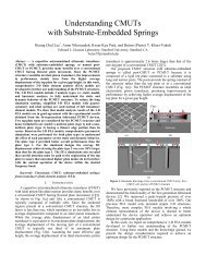
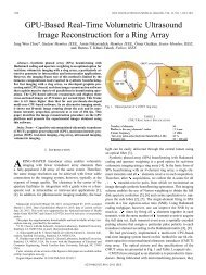
any intravascular ultrasound applicati<strong>on</strong>) the fr<strong>on</strong>t face of thetransducer should not c<strong>on</strong>tain any openings and it must bec<strong>on</strong>nected to ground and not to the hot electrode (large DCbias voltage). The reas<strong>on</strong>s for this are the requirement forgood signal to noise ratio, requiring a good grounding andshielding c<strong>on</strong>cept, and, even more important, human safety.Further, a flat c<strong>on</strong>tinuous transducer fr<strong>on</strong>t face, even for 1Dand 2D arrays, significantly simplifies any encapsulati<strong>on</strong> (e.g.Polydimethylsiloxane, Sylgard, etc.) and packaging (probe<str<strong>on</strong>g>fabricati<strong>on</strong></str<strong>on</strong>g>) task.Fifth, this process is ideal for implementing other CMUToperati<strong>on</strong> mode ideas, such as recently proposed in [6] and [7].For example, the idea of a CMUT with substrate-embeddedsprings for n<strong>on</strong>-flexural plate movement [7], requires a welldefinedlength of the vertical spring elements. The <strong>thick</strong>-BOXprocess inherently provides an etch stop, and, thus, guaranteesa c<strong>on</strong>stant spring element length over the entire wafer. In thisexample, <strong>on</strong>ly <strong>on</strong>e via through the <strong>thick</strong> BOX <strong>layer</strong> per CMUTelement would be required.Before describing our process flow, which fulfills all theserequirements, we will explain the background of the main idea.A closer look at the CMUT cell structure of a sacrificialrelease <str<strong>on</strong>g>based</str<strong>on</strong>g> device [Fig. 1(a)], compared to the structure ofa direct wafer-b<strong>on</strong>ded CMUT with single crystal silic<strong>on</strong> plate[Fig. 1(b)], illustrates a significant difference. For the waferb<strong>on</strong>deddevice with vacuum-sealed cavities and electricallyc<strong>on</strong>ductive silic<strong>on</strong> plate, the insulati<strong>on</strong> <strong>layer</strong> <strong>thick</strong>ness at thepost regi<strong>on</strong> is the limiting factor in terms of reliability (electricalbreakdown) and performance (parasitic capacitance). Thisis in particular the case for cell designs in which the gap heightis supposed to be small. Note that for most sacrificial releasedevices, the plate material is electrically insulating, i.e. a metalelectrode <strong>on</strong> top of the plate material is inevitable. Usingelectrically insulating materials, such as low-stress silic<strong>on</strong>nitride or nanocrystalline diam<strong>on</strong>d films, for the CMUT plateis feasible in wafer-b<strong>on</strong>ded CMUTs. However, this can becomechallenging in terms of b<strong>on</strong>d strength quality (yield) and cellto-celland element-to-element uniformity of such films whenused as CMUT plate material. Further, in many applicati<strong>on</strong>s,such as therapeutic ultrasound (e.g. high intensity focusedultrasound), the c<strong>on</strong>ductive (electrically and thermally) silic<strong>on</strong>plate is advantageous because no metal electrodes, as indicatedin [Fig. 1(b)], (except for ohmic c<strong>on</strong>tact points) are required.This is beneficial in terms of transducer heating, thermal stresseffects, and magnetic res<strong>on</strong>ance imaging tool compatibility.In previous work [5], we introduced the idea of extendingthe insulati<strong>on</strong> <strong>layer</strong> [Fig. 1(c)] into the substrate to address theaforementi<strong>on</strong>ed drawbacks (electrical breakdown and parasiticcapacitance). However, the questi<strong>on</strong> of how to incorporatesuch an improved cell structure into a 2D array process wasnot addressed by this approach. The basic questi<strong>on</strong> [Fig. 1(d)]we are facing here is how to realize a cell structure in whichthe high electric field (for high coupling efficiency and goodreceive sensitivity) is <strong>on</strong>ly applied where really needed – thegap regi<strong>on</strong> of the CMUT cell.One answer might be using an electrically insulating substrate,as suggested in [8]. This is indicated in Fig. 1(e).For example, fused silica <strong>on</strong> silic<strong>on</strong> wafers are commerciallyavailable for such endeavors, and advanced <strong>oxide</strong> etching of aBOX <strong>layer</strong> through a silic<strong>on</strong> via hole has been dem<strong>on</strong>strated[9].Instead of using an electrically insulating substrate, wepropose a silic<strong>on</strong>-<strong>on</strong>-insulati<strong>on</strong> (SOI) wafer as a substrate[Fig. 1(f)]. Such substrates are widely available (e.g. UltrasilCorporati<strong>on</strong>, Hayward, CA) with <strong>buried</strong> <strong>oxide</strong> (BOX) <strong>layer</strong><strong>thick</strong>nesses of up to several micr<strong>on</strong>s.A zoomed-in versi<strong>on</strong> [Fig. 1(g)] illustrates the idea inmore detail: In each evacuated cavity of the CMUT, verticalinsulati<strong>on</strong> trenches are used to form completely insulatedsilic<strong>on</strong> electrodes below the plate. According to the shownbiasing scheme (dc and ac), the high electric field <strong>on</strong>ly occursbelow each movable porti<strong>on</strong> of the plate. At the post regi<strong>on</strong>,however, the <strong>thick</strong> BOX <strong>layer</strong> gives additi<strong>on</strong>al protecti<strong>on</strong>against electrical breakdowns and, further, reduces the parasiticcapacitance. The hot electrode is fed through the <strong>thick</strong> BOX<strong>layer</strong> by using a doped polycrystalline silic<strong>on</strong> via or any otherelectrically c<strong>on</strong>ductive material, i.e. each cell has its ownindividual c<strong>on</strong>necti<strong>on</strong> to the hot electrode.Initially, we developed this idea for the <str<strong>on</strong>g>fabricati<strong>on</strong></str<strong>on</strong>g> ofCMUTs for high temperatures, in which very <strong>thick</strong> insulati<strong>on</strong><strong>layer</strong>s (reduced electrical breakdown voltages occur at elevatedtemperatures) are the key. Such a CMUT structure not <strong>on</strong>ly canbe fabricated very easily, it also features the <str<strong>on</strong>g>fabricati<strong>on</strong></str<strong>on</strong>g> of 1Dand 2D array c<strong>on</strong>figurati<strong>on</strong>s, which fulfill all aforementi<strong>on</strong>edrequirements for a versatile CMUT <str<strong>on</strong>g>fabricati<strong>on</strong></str<strong>on</strong>g> process.(a) (b) (c)(d)Thick BOX(e)(g) (h) (i)via holes(j) (k) (l)Fig. 2. Illustrati<strong>on</strong> of main <str<strong>on</strong>g>fabricati<strong>on</strong></str<strong>on</strong>g> steps. Only a small porti<strong>on</strong> of theCMUT is shown, i.e. <strong>on</strong>e quarter cell next to <strong>on</strong>e half cell of a neighboringCMUT element. Depending <strong>on</strong> the target frequency, the transducer c<strong>on</strong>figurati<strong>on</strong>(single element, 1D, 2D array), and the applicati<strong>on</strong>, some of these stepsare opti<strong>on</strong>al.(f)