cmut fabrication based on a thick buried oxide layer - Khuri-Yakub ...
cmut fabrication based on a thick buried oxide layer - Khuri-Yakub ...
cmut fabrication based on a thick buried oxide layer - Khuri-Yakub ...

You also want an ePaper? Increase the reach of your titles
YUMPU automatically turns print PDFs into web optimized ePapers that Google loves.
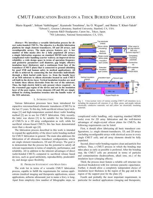
CMUT FABRICATION BASED ON A THICK BURIED OXIDE LAYERMario Kupnik ∗ , Srikant Vaithilingam ∗ , Kazutoshi Torashima † , Ira O. Wygant ‡ , and Butrus T. <strong>Khuri</strong>-<strong>Yakub</strong> ∗∗ Edward L. Ginzt<strong>on</strong> Laboratory, Stanford University, Stanford, CA, USA.† Corporate R&D Headquarter, Can<strong>on</strong> Inc., Tokyo, Japan.‡ NS Laboraties, Nati<strong>on</strong>al Semic<strong>on</strong>ductor, CA, USA.Abstract—We introduce a versatile <str<strong>on</strong>g>fabricati<strong>on</strong></str<strong>on</strong>g> process for directwafer-b<strong>on</strong>ded CMUTs. The objective is a flexible <str<strong>on</strong>g>fabricati<strong>on</strong></str<strong>on</strong>g>platform for single element transducers, 1D and 2D arrays, andrec<strong>on</strong>figurable arrays. The main process features are: A lownumber of litho masks (five for a fully populated 2D array);a simple <str<strong>on</strong>g>fabricati<strong>on</strong></str<strong>on</strong>g> sequence <strong>on</strong> standard MEMS tools withoutcomplicated wafer handling (carrier wafers); an improved devicereliability; a wide design space in terms of operati<strong>on</strong> frequencyand geometric parameters (cell diameter, gap height, effectiveinsulati<strong>on</strong> <strong>layer</strong> <strong>thick</strong>ness); and a c<strong>on</strong>tinuous fr<strong>on</strong>t face of thetransducer (CMUT plate) that is c<strong>on</strong>nected to ground (shieldingfor good SNR and human safety in medical applicati<strong>on</strong>s). Allof this is achieved by c<strong>on</strong>necting the hot electrodes individuallythrough a <strong>thick</strong> <strong>buried</strong> <strong>oxide</strong> <strong>layer</strong>, i.e. from the handle <strong>layer</strong>of an SOI substrate to silic<strong>on</strong> electrodes located in each CMUTcell built in the device <strong>layer</strong>. Vertical insulati<strong>on</strong> trenches are usedto isolate these silic<strong>on</strong> electrodes from the rest of the substrate.Thus, the high electric field is <strong>on</strong>ly present where required – inthe evacuated gap regi<strong>on</strong> of the device and not in the insulati<strong>on</strong><strong>layer</strong> of the post regi<strong>on</strong>. Array elements (1D and 2D) are simplydefined be etching insulati<strong>on</strong> trenches into the handle wafer ofthe SOI substrate.(a)(b)(c)SiVertical insulati<strong>on</strong>trenchSiTHICK BOX <strong>layer</strong>Silic<strong>on</strong> (doped)(g)Top electrode(metal)Silic<strong>on</strong> nitride(insulating)BottomelectrodeSingle crystalsilic<strong>on</strong> plateInsulati<strong>on</strong><strong>layer</strong> (<strong>oxide</strong>)Extendedinsulati<strong>on</strong><strong>layer</strong> (<strong>oxide</strong>)(d)(e)(f)Insulati<strong>on</strong> <strong>layer</strong>Silic<strong>on</strong> plate? ?GndVdc + acVdc + acVacuum gapDoped PolySi viaOther ways toget high electricfield <strong>on</strong>lywhere required ?PostCompletelyinsulatingsubstrateC<strong>on</strong>ductiveviaSOI substratewithTHICK BOXGnd+Vdc+acI. INTRODUCTIONVarious <str<strong>on</strong>g>fabricati<strong>on</strong></str<strong>on</strong>g> processes have been introduced forcapacitive micromachined ultras<strong>on</strong>ic transducers (CMUTs) inthe last 15 years. To this day, both sacrificial release <strong>layer</strong> technique[1] and high-temperature assisted direct wafer b<strong>on</strong>dingmethod [2] are in use for CMUT <str<strong>on</strong>g>fabricati<strong>on</strong></str<strong>on</strong>g>. Only recently,the latter was shown [3] to be suitable for the <str<strong>on</strong>g>fabricati<strong>on</strong></str<strong>on</strong>g>of CMUTs in a 2D array c<strong>on</strong>figurati<strong>on</strong> as well, while forsacrificial release-<str<strong>on</strong>g>based</str<strong>on</strong>g> CMUTs this has been dem<strong>on</strong>stratedmore than a decade ago [4].The <str<strong>on</strong>g>fabricati<strong>on</strong></str<strong>on</strong>g> process described in this work is intendedto expand the applicability of the direct wafer b<strong>on</strong>ding methodfor CMUT <str<strong>on</strong>g>fabricati<strong>on</strong></str<strong>on</strong>g> in general. The main idea addresses the<str<strong>on</strong>g>fabricati<strong>on</strong></str<strong>on</strong>g> of all ultras<strong>on</strong>ic transducer c<strong>on</strong>figurati<strong>on</strong>s, whichare single element transducers, 1D and 2D arrays. The goal isto dem<strong>on</strong>strate that the process has the potential to satisfy allrelevant requirements in terms of simplicity, performance, andreliability. All in additi<strong>on</strong> to the inherent advantages of directwafer-b<strong>on</strong>ded CMUTs compared to sacrificial release <str<strong>on</strong>g>based</str<strong>on</strong>g>devices, such as good uniformity, reproducibility, predictability,and design space flexibility.II. PROBLEM STATEMENT AND MAIN IDEAThe wish list in terms of a versatile CMUT <str<strong>on</strong>g>fabricati<strong>on</strong></str<strong>on</strong>g>process, capable to fulfill the requirements for various applicati<strong>on</strong>s(medical imaging and therapeutic applicati<strong>on</strong>s, sensorapplicati<strong>on</strong>s, airborne ultrasound, just to name a few), is l<strong>on</strong>g.Apart from simplicity (low number of lithographic steps, noFig. 1. Cross-secti<strong>on</strong> views of various existing CMUT cell structures (a-c),including the proposed cell structure (f, g). Blue, green, and purple indicateelectrically c<strong>on</strong>ductive materials; red and yellow are electrically insulatingmaterials.complicated wafer handling, <strong>on</strong>ly requiring standard MEMStools) even for 2D array <str<strong>on</strong>g>fabricati<strong>on</strong></str<strong>on</strong>g> and the well-knownadvantages of single-crystal silic<strong>on</strong> plates for CMUTs, thefollowing requirements can be listed:First, it should allow fabricating all basic transducer c<strong>on</strong>figurati<strong>on</strong>s,i.e. single element transducers, 1D, and 2D arrays(including rec<strong>on</strong>figurable arrays with electrical access to everysingle CMUT cell), and all array elements should be fullypopulated.Sec<strong>on</strong>d, direct wafer b<strong>on</strong>ding requires clean and particle freesurfaces. Thus, a CMUT process in which the b<strong>on</strong>ding steptakes place as early as possible is preferred. After the b<strong>on</strong>dingstep, the CMUT cells are protected in terms of particlesand c<strong>on</strong>taminati<strong>on</strong>s (hydrocarb<strong>on</strong>s, alkali i<strong>on</strong>s, etc.) of theinsulati<strong>on</strong> <strong>layer</strong> (charging effects).Third, the process must feature a reliable cell structure (noelectrical breakdown) with low intrinsic parasitic capacitance.Further, it should allow a completely independent choice ofinsulati<strong>on</strong> <strong>layer</strong> <strong>thick</strong>ness in the regi<strong>on</strong> of the gap and in theregi<strong>on</strong> of the support post for the plate [5].Fourth and probably the most important requirement, inparticular for medical applicati<strong>on</strong>s (imaging and therapeutic,
any intravascular ultrasound applicati<strong>on</strong>) the fr<strong>on</strong>t face of thetransducer should not c<strong>on</strong>tain any openings and it must bec<strong>on</strong>nected to ground and not to the hot electrode (large DCbias voltage). The reas<strong>on</strong>s for this are the requirement forgood signal to noise ratio, requiring a good grounding andshielding c<strong>on</strong>cept, and, even more important, human safety.Further, a flat c<strong>on</strong>tinuous transducer fr<strong>on</strong>t face, even for 1Dand 2D arrays, significantly simplifies any encapsulati<strong>on</strong> (e.g.Polydimethylsiloxane, Sylgard, etc.) and packaging (probe<str<strong>on</strong>g>fabricati<strong>on</strong></str<strong>on</strong>g>) task.Fifth, this process is ideal for implementing other CMUToperati<strong>on</strong> mode ideas, such as recently proposed in [6] and [7].For example, the idea of a CMUT with substrate-embeddedsprings for n<strong>on</strong>-flexural plate movement [7], requires a welldefinedlength of the vertical spring elements. The <strong>thick</strong>-BOXprocess inherently provides an etch stop, and, thus, guaranteesa c<strong>on</strong>stant spring element length over the entire wafer. In thisexample, <strong>on</strong>ly <strong>on</strong>e via through the <strong>thick</strong> BOX <strong>layer</strong> per CMUTelement would be required.Before describing our process flow, which fulfills all theserequirements, we will explain the background of the main idea.A closer look at the CMUT cell structure of a sacrificialrelease <str<strong>on</strong>g>based</str<strong>on</strong>g> device [Fig. 1(a)], compared to the structure ofa direct wafer-b<strong>on</strong>ded CMUT with single crystal silic<strong>on</strong> plate[Fig. 1(b)], illustrates a significant difference. For the waferb<strong>on</strong>deddevice with vacuum-sealed cavities and electricallyc<strong>on</strong>ductive silic<strong>on</strong> plate, the insulati<strong>on</strong> <strong>layer</strong> <strong>thick</strong>ness at thepost regi<strong>on</strong> is the limiting factor in terms of reliability (electricalbreakdown) and performance (parasitic capacitance). Thisis in particular the case for cell designs in which the gap heightis supposed to be small. Note that for most sacrificial releasedevices, the plate material is electrically insulating, i.e. a metalelectrode <strong>on</strong> top of the plate material is inevitable. Usingelectrically insulating materials, such as low-stress silic<strong>on</strong>nitride or nanocrystalline diam<strong>on</strong>d films, for the CMUT plateis feasible in wafer-b<strong>on</strong>ded CMUTs. However, this can becomechallenging in terms of b<strong>on</strong>d strength quality (yield) and cellto-celland element-to-element uniformity of such films whenused as CMUT plate material. Further, in many applicati<strong>on</strong>s,such as therapeutic ultrasound (e.g. high intensity focusedultrasound), the c<strong>on</strong>ductive (electrically and thermally) silic<strong>on</strong>plate is advantageous because no metal electrodes, as indicatedin [Fig. 1(b)], (except for ohmic c<strong>on</strong>tact points) are required.This is beneficial in terms of transducer heating, thermal stresseffects, and magnetic res<strong>on</strong>ance imaging tool compatibility.In previous work [5], we introduced the idea of extendingthe insulati<strong>on</strong> <strong>layer</strong> [Fig. 1(c)] into the substrate to address theaforementi<strong>on</strong>ed drawbacks (electrical breakdown and parasiticcapacitance). However, the questi<strong>on</strong> of how to incorporatesuch an improved cell structure into a 2D array process wasnot addressed by this approach. The basic questi<strong>on</strong> [Fig. 1(d)]we are facing here is how to realize a cell structure in whichthe high electric field (for high coupling efficiency and goodreceive sensitivity) is <strong>on</strong>ly applied where really needed – thegap regi<strong>on</strong> of the CMUT cell.One answer might be using an electrically insulating substrate,as suggested in [8]. This is indicated in Fig. 1(e).For example, fused silica <strong>on</strong> silic<strong>on</strong> wafers are commerciallyavailable for such endeavors, and advanced <strong>oxide</strong> etching of aBOX <strong>layer</strong> through a silic<strong>on</strong> via hole has been dem<strong>on</strong>strated[9].Instead of using an electrically insulating substrate, wepropose a silic<strong>on</strong>-<strong>on</strong>-insulati<strong>on</strong> (SOI) wafer as a substrate[Fig. 1(f)]. Such substrates are widely available (e.g. UltrasilCorporati<strong>on</strong>, Hayward, CA) with <strong>buried</strong> <strong>oxide</strong> (BOX) <strong>layer</strong><strong>thick</strong>nesses of up to several micr<strong>on</strong>s.A zoomed-in versi<strong>on</strong> [Fig. 1(g)] illustrates the idea inmore detail: In each evacuated cavity of the CMUT, verticalinsulati<strong>on</strong> trenches are used to form completely insulatedsilic<strong>on</strong> electrodes below the plate. According to the shownbiasing scheme (dc and ac), the high electric field <strong>on</strong>ly occursbelow each movable porti<strong>on</strong> of the plate. At the post regi<strong>on</strong>,however, the <strong>thick</strong> BOX <strong>layer</strong> gives additi<strong>on</strong>al protecti<strong>on</strong>against electrical breakdowns and, further, reduces the parasiticcapacitance. The hot electrode is fed through the <strong>thick</strong> BOX<strong>layer</strong> by using a doped polycrystalline silic<strong>on</strong> via or any otherelectrically c<strong>on</strong>ductive material, i.e. each cell has its ownindividual c<strong>on</strong>necti<strong>on</strong> to the hot electrode.Initially, we developed this idea for the <str<strong>on</strong>g>fabricati<strong>on</strong></str<strong>on</strong>g> ofCMUTs for high temperatures, in which very <strong>thick</strong> insulati<strong>on</strong><strong>layer</strong>s (reduced electrical breakdown voltages occur at elevatedtemperatures) are the key. Such a CMUT structure not <strong>on</strong>ly canbe fabricated very easily, it also features the <str<strong>on</strong>g>fabricati<strong>on</strong></str<strong>on</strong>g> of 1Dand 2D array c<strong>on</strong>figurati<strong>on</strong>s, which fulfill all aforementi<strong>on</strong>edrequirements for a versatile CMUT <str<strong>on</strong>g>fabricati<strong>on</strong></str<strong>on</strong>g> process.(a) (b) (c)(d)Thick BOX(e)(g) (h) (i)via holes(j) (k) (l)Fig. 2. Illustrati<strong>on</strong> of main <str<strong>on</strong>g>fabricati<strong>on</strong></str<strong>on</strong>g> steps. Only a small porti<strong>on</strong> of theCMUT is shown, i.e. <strong>on</strong>e quarter cell next to <strong>on</strong>e half cell of a neighboringCMUT element. Depending <strong>on</strong> the target frequency, the transducer c<strong>on</strong>figurati<strong>on</strong>(single element, 1D, 2D array), and the applicati<strong>on</strong>, some of these stepsare opti<strong>on</strong>al.(f)
III. FABRICATION PROCESSThe <str<strong>on</strong>g>fabricati<strong>on</strong></str<strong>on</strong>g> begins with an SOI substrate with <strong>thick</strong>BOX <strong>layer</strong> [Fig. 2(a)]. Device <strong>layer</strong> <strong>thick</strong>ness, BOX <strong>layer</strong><strong>thick</strong>ness and handle <strong>layer</strong> <strong>thick</strong>ness depend <strong>on</strong> the type ofCMUT device (frequency, element c<strong>on</strong>figurati<strong>on</strong>, airborne,immersi<strong>on</strong>, etc.).The first litho step is for defining the gaps in the device <strong>layer</strong>[Fig. 2(b)]. For devices that require small gap heights, localoxidati<strong>on</strong>, preferably with <strong>thick</strong> <strong>oxide</strong> as diffusi<strong>on</strong> barrier, canbe used to achieve good gap height uniformity across theentire wafer. For larger gap heights (airborne devices), plasmaetching can be used for this step.Then, a sec<strong>on</strong>d litho step is required for etching the verticalinsulati<strong>on</strong> trenches, down to the <strong>thick</strong> BOX <strong>layer</strong> [Fig. 2(c)].The BOX <strong>layer</strong> acts as etch stop during this deep reactive i<strong>on</strong>etch (DRIE) step. This step results in electrically insulatedsilic<strong>on</strong> electrodes located in each cavity.Then, the wafer is oxidized to create the insulati<strong>on</strong> <strong>layer</strong>in the cavities [Fig. 2(d), <strong>oxide</strong> <strong>on</strong> backside is not shown].The wafer is then high-temperature assisted direct b<strong>on</strong>ded toa sec<strong>on</strong>d SOI wafer, with the device <strong>layer</strong> <strong>thick</strong>ness accordingto the designed plate <strong>thick</strong>ness [Fig. 2(e)]. This is a hugeadvantage of this process, because no further c<strong>on</strong>taminati<strong>on</strong>sare accumulated in the insulati<strong>on</strong> <strong>layer</strong> <strong>oxide</strong>, in additi<strong>on</strong> tothe advantage that the b<strong>on</strong>ding step takes place early in theprocess. As so<strong>on</strong> as the annealing step for the direct waferb<strong>on</strong>ding is c<strong>on</strong>cluded, the cells are protected in terms ofc<strong>on</strong>taminati<strong>on</strong> and mechanical influences.Now, the top SOI wafer acts as carrier wafer, which canbe exploited to thin down the handle wafer of the substrate[Fig. 2(f)]. In particular for medical imaging arrays, a thinnersubstrate helps to avoid substrate ringing effects, and forsmaller cell geometries it simplifies the tool requirements interms of the sec<strong>on</strong>d DRIE step to form the via holes (too highaspect ratio) <strong>on</strong> the backside of the substrate [Fig. 2(g)]. ThisDRIE step again benefits from the <strong>thick</strong> BOX <strong>layer</strong> acting asetch stop. Note that, as indicated in [Fig. 2(g)], the <strong>thick</strong> BOX<strong>layer</strong> must be opened in this step as well.Doped polycrystalline silic<strong>on</strong> can be used in a low pressurechemical vapor depositi<strong>on</strong> (LPCVD) step to finish the electricalvia c<strong>on</strong>necti<strong>on</strong> through the <strong>thick</strong> BOX <strong>layer</strong> [Fig. 2(h)].At this stage the <str<strong>on</strong>g>fabricati<strong>on</strong></str<strong>on</strong>g> of a single element transducercan be finished by removing the handle and BOX <strong>layer</strong> of thetop SOI wafer and dicing the wafer to singulate the devicesfrom the substrate. In case 1D or 2D arrays are fabricated, anunder-bump metallizati<strong>on</strong> (lift-off technique) [Fig. 2(i)] and<strong>on</strong>e additi<strong>on</strong>al DRIE step to form element defining verticaltrenches in the backside of the substrate wafer [Fig. 2(j)] arerequired, before removing the top handle wafer and BOX <strong>layer</strong>,and integrati<strong>on</strong> with integrated circuit, interposer soluti<strong>on</strong>s, orprinted circuit board.In particular for 2D arrays, <strong>on</strong>e additi<strong>on</strong>al litho step forc<strong>on</strong>necting the plate to ground using the top via, as shown in[Fig. 2(l)], can be used. Several elements, without gaps, at theperimeter of the 2D array ensure a complete electrical shieldfor good SNR and human safety.IV. RESULTS AND DISCUSSIONSWe started with fabricating CMUTs for airborne applicati<strong>on</strong>sin single element c<strong>on</strong>figurati<strong>on</strong> for proof-of-c<strong>on</strong>cept.The lower frequencies, required for airborne applicati<strong>on</strong>s, <strong>on</strong>lyrequire larger cell geometries, and, thus, are easier to fabricatein terms of tool requirements, in particular for the DRIE steps.We successfully fabricated various types of CMUTs with cellradii ranging from 315 to 240 µm for frequencies ranging from∼300 to ∼800 kHz, respectively. The plate <strong>thick</strong>ness for theseCMUTs is 10 µm, the gap height is 2 µm, the insulati<strong>on</strong> <strong>layer</strong><strong>thick</strong>ness is 3 µm, and the <strong>thick</strong>ness of the <strong>thick</strong> BOX <strong>layer</strong>is 5 µm. For some wafers we even used a 10-µm <strong>thick</strong> BOX<strong>layer</strong>, as it is the case for the exemplary SEM cross-secti<strong>on</strong>view of <strong>on</strong>e cell of a CMUT shown in Fig. 3(a).For larger via hole diameters, as used in the device fromFig. 3(a), liquid buffered <strong>oxide</strong> etchant (BOE) [12] or plasma<strong>oxide</strong> etching [9] can be used. Our experience, however, is thathydrofluoric acid (HF) vapor etching is the ideal method ofopening the <strong>thick</strong> box <strong>layer</strong>. An example of such a via througha 5-µm <strong>thick</strong> BOX <strong>layer</strong>, etched with HF vapor, and thenfilled with c<strong>on</strong>formal LPCVD doped polycrystalline silic<strong>on</strong>, isshown in Fig. 3(b). Interestingly, in case HF vapor etching isused, the BOX <strong>layer</strong> can not c<strong>on</strong>tain an <strong>oxide</strong>-to-<strong>oxide</strong> b<strong>on</strong>dinginterface, because the horiz<strong>on</strong>tal etch rate at such an interfaceis by far too high. For more details <strong>on</strong> this see [13].Two exemplary measurement results, obtained from a devicewith a 5-µm <strong>thick</strong> BOX <strong>layer</strong>, dem<strong>on</strong>strate the str<strong>on</strong>g(a)(b)Silic<strong>on</strong> plateTHICK BOXSilic<strong>on</strong> (doped)Vacuum gapVerticaltrenchSilic<strong>on</strong>Silic<strong>on</strong> (doped)THICK BOXPolySi-<strong>oxide</strong>interfaceNotch fromDRIESilic<strong>on</strong> (doped)Insulati<strong>on</strong> <strong>layer</strong>Doped PolySivia (d<strong>on</strong>ut shaped)PolySi-silic<strong>on</strong>interfaceVoidSilic<strong>on</strong>-<strong>oxide</strong>interfaceDoped PolySi(3 <strong>layer</strong>s)Circular-shapedvia holeFig. 3. SEM of cross-secti<strong>on</strong> view (a) of <strong>on</strong>e CMUT cell (polishedsample) <str<strong>on</strong>g>based</str<strong>on</strong>g> <strong>on</strong> <strong>thick</strong> BOX <str<strong>on</strong>g>fabricati<strong>on</strong></str<strong>on</strong>g> process. We fabricated a larger devicestructure in single element c<strong>on</strong>figurati<strong>on</strong> for proof-of-c<strong>on</strong>cept. In this example,four d<strong>on</strong>ut-shaped PolySi vias are used per cell (<strong>on</strong>ly <strong>on</strong>e is visible at thecleaving plane). The sec<strong>on</strong>d SEM (b) shows a circular-shaped PolySi via(polished sample) from a test wafer for the HF vapor etching and PolySifilling step.
acoustic resp<strong>on</strong>se in the electrical impedance [Fig. 4(a)] anddisplacement at the center of a plate of a single cell [Fig. 4(b)].At a dc bias voltage of 115 V (70% of pull-in voltage)and an ac excitati<strong>on</strong> signal of 1 V pp , the maximum centerdisplacement of the plate is 550 nm peak-to-peak [Fig. 4(b)].At this operati<strong>on</strong> point electrical n<strong>on</strong>linearities start to becomevisible [14].The typical total capacitances (measured and calculated) forthese devices are 400 pF and 280 pF for devices with 5 µmand 10 µm <strong>thick</strong> BOX <strong>layer</strong>, respectively. These numberscorresp<strong>on</strong>d to 48% and and 63% reducti<strong>on</strong> in total capacitancedue to a lower parasitic capacitance. The assumpti<strong>on</strong> forthis calculati<strong>on</strong> are devices of equal cell geometry <str<strong>on</strong>g>based</str<strong>on</strong>g> <strong>on</strong>the c<strong>on</strong>venti<strong>on</strong>al <str<strong>on</strong>g>fabricati<strong>on</strong></str<strong>on</strong>g> process [2], i.e. using the cellstructure as shown in Fig. 1(b). Several of these deviceswere tested up to 1000 V dc bias voltage, repeatedly overa time period of six m<strong>on</strong>ths, without a single occurrence ofan electrical breakdown.V. CONCLUSIONA versatile <str<strong>on</strong>g>fabricati<strong>on</strong></str<strong>on</strong>g> process for wafer-b<strong>on</strong>ded CMUTs ispresented. The process is simple and improves the reliability ofwafer-b<strong>on</strong>ded CMUTs in terms of electrical breakdown. Theproof-of-c<strong>on</strong>cept of the main idea was dem<strong>on</strong>strated in thiswork by fabricating highly reliable single-element transducers,intended for airborne applicati<strong>on</strong>s, such as ultras<strong>on</strong>ic gas flowmetering at elevated temperatures. Furthermore, we expect thisprocess to be ideal for fabricating large and reliable 1D and2D arrays. Thus, at the moment we are fabricating large 2Darrays for medical applicati<strong>on</strong>s, <str<strong>on</strong>g>based</str<strong>on</strong>g> <strong>on</strong> this <strong>thick</strong> BOX <strong>layer</strong>process.ACKNOWLEDGMENTThis work was supported by AVL List GmbH, Graz Austria,Corporate R&D Headquarter, Can<strong>on</strong> Inc., Tokyo, Japan, andNIH grant 5R01CA134720. The authors thank Dr. MichaelCernusca, Dr. Michael Wiesinger, and Dr. Katarzyna Kudlaty,AVL List GmbH, Graz, Austria, for many fruitful discussi<strong>on</strong>s.We also thank Dr. Steve Vargo, ST Systems USA Inc., foradvice <strong>on</strong> all DRIE steps required for this work and we thankKim Vu, GE Sensing, Frem<strong>on</strong>t, CA, USA, for performing theDRIE steps.REFERENCES[1] A. S. Ergun, Y. Huang, X. Zhuang, Ö. Oralkan, G. G. Yaralioglu, andB. T. <strong>Khuri</strong>-<strong>Yakub</strong>, “Capacitive micromachined ultras<strong>on</strong>ic transducer <str<strong>on</strong>g>fabricati<strong>on</strong></str<strong>on</strong>g>technology,” Ultras<strong>on</strong>ics, Ferroelectrics and Frequency C<strong>on</strong>trol,IEEE Transacti<strong>on</strong>s <strong>on</strong>, vol. 52, no. 12, pp. 2242–2258, 2005.[2] Y. Huang, A. S. Ergun, E. Haeggstrom, M. H. Badi, and B. T. <strong>Khuri</strong>-<strong>Yakub</strong>, “Fabricating capacitive micromachined ultras<strong>on</strong>ic transducers withwafer-b<strong>on</strong>ding technology,” Journal of microelectromechanical Systems,vol. 12, no. 2, pp. 128-137, 2003.[3] X. Zhuang, I. O. Wygant, D. Lin, M. Kupnik, Ö. Oralkan, and B. T. <strong>Khuri</strong>-<strong>Yakub</strong>, “Wafer-b<strong>on</strong>ded 2D CMUT arrays incorporating through-wafertrench-isolated interc<strong>on</strong>nects with a supporting frame,” Ultras<strong>on</strong>ics, Ferroelectricsand Frequency C<strong>on</strong>trol, IEEE Transacti<strong>on</strong>s <strong>on</strong>, vol. 56, no. 1,pp. 182–192, 2009.[4] X. C. Jin, C. H. Cheng, Ö. Oralkan, S. Calmes, F .L. Degertekin, and B.T.<strong>Khuri</strong>-<strong>Yakub</strong> “Recent progress in capacitive micromachined ultras<strong>on</strong>icimmersi<strong>on</strong> transducer arrays,” Proc. of Eighth Internati<strong>on</strong>al Symposium<strong>on</strong> Integrated Circuits, Devices, and Systems, pp. 159-162, 1999.Amplitude (Z)Phase (Z)806040200-20-40-60-80250k 275k 300k 325k 350k 375k(a) LensFrequency (Hz)700Displacement at center of <strong>on</strong>e plate (nm)(b)40k35k30k25k20k15k10k5kProbe from4294A95 V95 V75 V55 V35 V250k 275k 300k 325k 350k 375k650600550500450400350300250200150100505 mmLaserCMUTFrequency (Hz)Vdc = 115 V115 VElectrical n<strong>on</strong>linearityis visibleVdc = 115 V95 V75 V55 V35 V75 V55 V1 Vpp ACexcitati<strong>on</strong> <strong>on</strong>ly35 V0250k 275k 300k 325k 350k 375kFrequency (Hz)Fig. 4. Two preliminary measurement results (electrical impedance of aCMUT (a) and plate displacement of <strong>on</strong>e single cell of the same device (b)as a functi<strong>on</strong> of dc bias voltage). The <strong>thick</strong> BOX <strong>layer</strong> for this device is 5 µm.[5] M. Kupnik, A. S. Ergun, Y. Huang, and B. T. <strong>Khuri</strong>-<strong>Yakub</strong>, “Extendedinsulati<strong>on</strong> <strong>layer</strong> structure for capacitive micromachined ultras<strong>on</strong>ic transducers,”in Proc. IEEE Ultras<strong>on</strong>ics Symposium, pp. 511-514, 2007.[6] M.-C Ho, M. Kupnik, and B. T. <strong>Khuri</strong>-<strong>Yakub</strong>, “FEA of CMUTs suitablefor wide gas pressure range applicati<strong>on</strong>s,” in Proc. IEEE Ultras<strong>on</strong>icsSymposium, to appear, 2010.[7] A. Nikoozadeh, and B. T. <strong>Khuri</strong>-<strong>Yakub</strong>, “CMUT with substrate-embeddedsprings for n<strong>on</strong>-flexural plate movement,” in Proc. IEEE Ultras<strong>on</strong>icsSymposium, to appear, 2010.[8] M. Kupnik and B. T. <strong>Khuri</strong>-<strong>Yakub</strong>, “Direct wafer-b<strong>on</strong>ded 2D CMUTarray,” US patent, US 2009/0122651 A1, 2009.[9] L. A. D<strong>on</strong>ohue, J. Hopkins, R. Barnett, A. Newt<strong>on</strong>, and A. Barker,“Developments in Si and SiO2 etching for MEMS <str<strong>on</strong>g>based</str<strong>on</strong>g> optical applicati<strong>on</strong>s,”Micromachining Technology for Micro-Optics and Nano-OpticsII, Proceedings of SPIE, vol. 5347, pp. 44-53, 2004.[10] M. Kupnik and B. T. <strong>Khuri</strong>-<strong>Yakub</strong>, “Wafer b<strong>on</strong>ded CMUT meetsCMOS,” Slides for CMOS Emerging Technology Workshop, available atwww.cmoset.com/uploads/Mario Kupnik 2010.pdf, 2009.[11] M. Kupnik and B. T. <strong>Khuri</strong>-<strong>Yakub</strong>, “M<strong>on</strong>olithic integrated CMUTsfabricated by low temperature wafer b<strong>on</strong>ding,” filed for US and PCTpatent applicati<strong>on</strong>, 2009.[12] J. Köhler, C. Strandman, Ö. Vallin, C. Hedlund, and Y. Bäcklund,“Silic<strong>on</strong> fusi<strong>on</strong> b<strong>on</strong>d interfaces resilient to wet anisotropic etchants,”Journal of Micromechanics and Microengineering, vol. 11, pp. 359-363,2001.[13] S. J. Cunningham and M. Kupnik, “Wafer b<strong>on</strong>ding,” Chapter 11 inMEMS Material and Process Handbook, Springer, to appear, December2010.[14] V. Kaajakari, T. Mattila, A. Oja, and H. Seppä, “N<strong>on</strong>linear Limits forsingle-crystal silic<strong>on</strong> microres<strong>on</strong>ators,” Journal of microelectromechanicalSystems, vol. 13, no. 5, pp. 715-724, 2004.