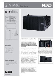
- Page 1 and 2:
SERVICE MANUAL■ CONTENTS PANEL LA
- Page 3 and 4:
NXAMP4x4■ PANEL LAYOUT • Front
- Page 5 and 6:
NXAMP4x4■ SERVICE PRECAUTIONS Saf
- Page 7 and 8:
NXAMP4x4■ OVERALL ASSEMBLY WIRING
- Page 9 and 10:
NXAMP4x43. Wiring of the FANConnect
- Page 11 and 12:
NXAMP4x4d, e) Fix the wires to the
- Page 13 and 14:
NXAMP4x4CN401YELLOW Fig. 20 NOTE:
- Page 15 and 16:
NXAMP4x4b-3) Then fasten these wire
- Page 17 and 18:
NXAMP4x4At the stage as shown in Fi
- Page 19 and 20:
NXAMP4x4o) Fasten the wires (WK0208
- Page 21 and 22:
NXAMP4x48. Color of the connectors
- Page 23 and 24:
NXAMP4x412. Confirmation of Switch
- Page 25 and 26:
NXAMP4x4■ DISASSEMBLY PROCEDURES
- Page 27 and 28:
NXAMP4x43. PSANHA Circuit Board(Tim
- Page 29 and 30:
NXAMP4x45. PSANHB Circuit Board(Tim
- Page 31 and 32:
NXAMP4x48. Upper left (CH1) PA unit
- Page 33 and 34:
NXAMP4x412. Front Panel Assembly(Ti
- Page 35 and 36:
NXAMP4x416. Lower left DC Fan(Time
- Page 37 and 38:
■ LSI PIN DESCRIPTION NXAMP4x4
- Page 39 and 40:
NXAMP4x4CS4272-CZZR (X8487A0)CODECC
- Page 41 and 42:
NXAMP4x4NJU7630-M (X8682A0)Regulato
- Page 43 and 44:
NXAMP4x4SN74LVC157APWR (X6786A0)Dat
- Page 45 and 46:
NXAMP4x4• INANH Circuit Boardto C
- Page 47 and 48:
NXAMP4x4• CONTROL Circuit BoardAA
- Page 49 and 50:
NXAMP4x4• CONTROL Circuit BoardBP
- Page 51 and 52:
NXAMP4x4• OUTANH Circuit BoardPat
- Page 53 and 54:
NXAMP4x4• PN-AN Circuit BoardAEnc
- Page 55 and 56:
NXAMP4x4• PN-AN Circuit BoardBPat
- Page 57 and 58:
NXAMP4x4• PAANH Circuit BoardAA't
- Page 59 and 60:
NXAMP4x4• PSANHA, PSANHB Circuit
- Page 61 and 62:
NXAMP4x4• PSANHA, PSANHB Circuit
- Page 63 and 64:
NXAMP4x4• NX-DFLT Circuit BoardEx
- Page 65 and 66:
NXAMP4x43. Operation3-1. Entry of t
- Page 67 and 68:
NXAMP4x4Switch the GPI jig to the G
- Page 69 and 70:
NXAMP4x44-15. ANALOG testPress the
- Page 71 and 72:
NXAMP4x4■ 71
- Page 73 and 74:
NXAMP4x4 73
- Page 75 and 76:
NXAMP4x4 7
- Page 77 and 78:
NXAMP4x4
- Page 79 and 80:
NXAMP4x41-5. Other0 dBu is defined
- Page 81 and 82:
NXAMP4x44-7. Channel separation1) G
- Page 83 and 84:
NXAMP4x4■
- Page 85 and 86:
NXAMP4x4
- Page 87 and 88: NXAMP4x4
- Page 89 and 90: NXAMP4x45) Click the [Create] butto
- Page 91 and 92: NXAMP4x4 91
- Page 93 and 94: NXAMP4x4■ OVERALL ASSEMBLY 1/2 8
- Page 95 and 96: NXAMP4x4■ OVERALL ASSEMBLY 2/2 2
- Page 97 and 98: NXAMP4x4REF NO. PART NO. DESCRIPTIO
- Page 99 and 100: NXAMP4x4REF NO. PART NO. DESCRIPTIO
- Page 101 and 102: NXAMP4x4■ LOCATIONS OF HEAT SINK
- Page 103 and 104: NXAMP4x4■ HEAT SINK UNIT L100 PS
- Page 105 and 106: NXAMP4x4■ HEAT SINK UNIT L60 PSA
- Page 107 and 108: NXAMP4x4■ HEAT SINK UNIT L50 PSA
- Page 109 and 110: NXAMP4x4■ HEAT SINK UNIT MP-5 PA
- Page 111 and 112: NXAMP4x4■ ELECTRICAL PARTS REF NO
- Page 113 and 114: NXAMP4x4REF NO. PART NO. DESCRIPTIO
- Page 115 and 116: NXAMP4x4CONTROLREF NO. PART NO. DES
- Page 117 and 118: NXAMP4x4REF NO. PART NO. DESCRIPTIO
- Page 119 and 120: NXAMP4x4REF NO. PART NO. DESCRIPTIO
- Page 121 and 122: NXAMP4x4REF NO. PART NO. DESCRIPTIO
- Page 123 and 124: NXAMP4x4PAANHREF NO. PART NO. DESCR
- Page 125 and 126: NXAMP4x4REF NO. PART NO. DESCRIPTIO
- Page 127 and 128: NXAMP4x4REF NO. PART NO. DESCRIPTIO
- Page 129 and 130: NXAMP4x4REF NO. PART NO. DESCRIPTIO
- Page 131 and 132: NXAMP4x4CIRCUIT DIAGRAM■ CONTENTS
- Page 133 and 134: KJIHGFEDCBANXAMP4x4■ WIRING DIAGR
- Page 135 and 136: HGFEDCBANXAMP4x4■ BLOCK DIAGRAM 2
- Page 137: HGFEDCBANXAMP4x4■ BLOCK DIAGRAM 4
- Page 141 and 142: QPONMLKJIHGFEDCBANXAMP4x4■ CIRCUI
- Page 143 and 144: QPONMLKJIHGFEDCBANXAMP4x4■ CIRCUI
- Page 145 and 146: HGFEDCBANXAMP4x4■ CIRCUIT DIAGRAM
- Page 147 and 148: QPONMLKJIHGFEDCBANXAMP4x4■ CIRCUI
- Page 149 and 150: LKJIHGFEDCBANXAMP4x4■ CIRCUIT DIA
- Page 151 and 152: LKJIHGFEDCBANXAMP4x4■ CIRCUIT DIA
- Page 153: QPONMLKJIHGFEDCBANXAMP4x4■ CIRCUI