Research Journal of Science & IT Management - RJSITM - The ...
Research Journal of Science & IT Management - RJSITM - The ...
Research Journal of Science & IT Management - RJSITM - The ...

Create successful ePaper yourself
Turn your PDF publications into a flip-book with our unique Google optimized e-Paper software.
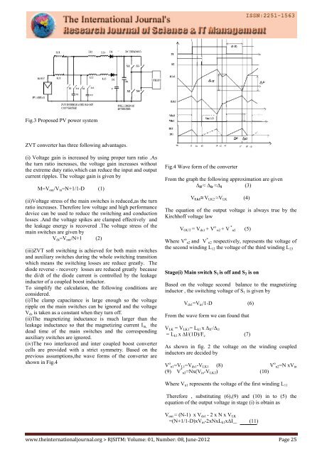
Fig.3 Proposed PV power system<br />
ZVT converter has three following advantages.<br />
(i) Voltage gain is increased by using proper turn ratio .As<br />
the turn ratio increases, the voltage gain increases without<br />
the extreme duty ratio,which can reduce the input and output<br />
current ripples. <strong>The</strong> voltage gain is given by<br />
M=V out /V in =N+1/1-D (1)<br />
(ii)Voltage stress <strong>of</strong> the main switches is reduced,as the turn<br />
ratio increases. <strong>The</strong>refore low voltage and high performance<br />
device can be used to reduce the switching and conduction<br />
losses .And the voltage spikes are clamped effectively and<br />
the leakage energy is recovered .<strong>The</strong> voltage stress <strong>of</strong> the<br />
main switches are given by<br />
V ds =V out /N+1 (2)<br />
(iii)ZVT s<strong>of</strong>t switching is achieved for both main switches<br />
and auxiliary switches during the whole switching transition<br />
which means the switching losses are reduce greatly. <strong>The</strong><br />
diode reverse - recovery losses are reduced greatly because<br />
the di/dt <strong>of</strong> the diode current is controlled by the leakage<br />
inductor <strong>of</strong> a coupled boost inductor.<br />
To simplify the calculation, the following conditions are<br />
considered.<br />
(i)<strong>The</strong> clamp capacitance is large enough so the voltage<br />
ripple on the main switches can be ignored and the voltage<br />
V ds is taken as a constant when they turn <strong>of</strong>f.<br />
(ii)<strong>The</strong> magnetizing inductance is much larger than the<br />
leakage inductance so that the magnetizing current I m, the<br />
dead time <strong>of</strong> the main switches and the corresponding<br />
auxiliary switches are ignored.<br />
(iv)<strong>The</strong> two interleaved and inter coupled boost converter<br />
cells are provided with a strict symmetry. Based on the<br />
previous assumptions,the wave forms <strong>of</strong> the converter are<br />
shown in Fig.4<br />
Fig.4 Wave form <strong>of</strong> the converter<br />
From the graph the following approximation are given<br />
∆ If ≈ ∆ Ir ≈∆ I (3)<br />
V Lk1 ≈ V LK2 ≈V LK (4)<br />
<strong>The</strong> equation <strong>of</strong> the output voltage is always true by the<br />
Kirchh<strong>of</strong>f voltage law<br />
V OUT = V ds1 + V o n2 + V * n2 (5)<br />
Where V o n2 and V * n2 respectively, represents the voltage <strong>of</strong><br />
the second winding L 12 the voltage <strong>of</strong> the third winding L 23<br />
Stage(i) Main switch S 1 is <strong>of</strong>f and S 2 is on<br />
Based on the voltage second balance to the magnetizing<br />
inductor , the switching voltage <strong>of</strong> S 1 is given by<br />
V ds1 =V in /1-D (6)<br />
From the wave form we can found that<br />
V LK = V LK1 = L k1 x ∆ If /∆ t1<br />
= L k1 x ∆I/(1D)/F c (7)<br />
As shown in fig. 2 the voltage on the winding coupled<br />
inductors are decided by<br />
V o n1=V L1 =V ds1 -V LK1 (8) V o n2=N xV in<br />
(9) V * n2=Nx(V in -V LK2 ) (10)<br />
Where V n1 represents the voltage <strong>of</strong> the first winding L 11<br />
<strong>The</strong>refore , substituting (6),(9) and (10) in to (5) the<br />
equation <strong>of</strong> the output voltage in stage (i) is obtain as<br />
V out = (N-1) x V ds1 - 2 x N x V LK<br />
=(N+1/1-D)xV in -2xNxL k1 x∆I (11)<br />
www.theinternationaljournal.org > RJS<strong>IT</strong>M: Volume: 01, Number: 08, June-2012 Page 25