Annual report 2009 - Imec
Annual report 2009 - Imec
Annual report 2009 - Imec

You also want an ePaper? Increase the reach of your titles
YUMPU automatically turns print PDFs into web optimized ePapers that Google loves.
hIGhLIGhTs<br />
IMEC CORE CMOS<br />
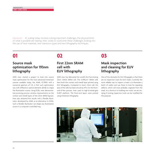
HIgHLIgHTS - IC scaling today involves solving important challenges; the physical limits<br />
of what is possible are nearing. <strong>Imec</strong> works to overcome these challenges, looking into<br />
the use of new materials, new transistor types and new lithography techniques.<br />
01<br />
Source mask<br />
optimization for 193nm<br />
lithography<br />
<strong>2009</strong>, imec started a project to look into source<br />
mask optimization for the most advanced immersion<br />
scanner available today, the ASML XT:1900i with a<br />
numerical aperture of 1.35. A first such optimization<br />
was with diffractive optical elements (DOE) to shape<br />
the illumination source. Using DOEs, imec demonstrated<br />
promising process window improvements on the<br />
contact and metal1 layers of the 22nm SRAM layouts.<br />
<strong>Imec</strong> also obtained first results with a flexible illuminator,<br />
developed by ASML as an alternative to DOEs.<br />
Such a flexible illuminator can shape any illumination<br />
source in a computer-controlled way.<br />
24<br />
02<br />
First 22nm SRAM<br />
cell with<br />
EUV lithography<br />
<strong>2009</strong>, imec has fabricated the world’s first functioning<br />
22nm CMOS SRAM cell. The 0.099µm² SRAM cells<br />
have both the contact and metal1 layer printed using<br />
EUV lithography. Compared to imec’s 32nm cell, the<br />
area of the cells has been shrunk by 47%. For the frontend-of-line<br />
process, imec used its high-k/metal-gate<br />
FinFET platform. The front-end layers were printed<br />
using immersion lithography.<br />
03<br />
Mask inspection<br />
and cleaning for EUV<br />
lithography<br />
One of the obstacles for EUV lithography is that there<br />
are no inspection tools for EUV masks. Currently the<br />
most reliable way to inspect a mask is to illuminate a<br />
batch of wafers and use these to look for repeating<br />
defects, which will most probably originate from the<br />
mask. As a shortcut to building new tools, we are studying<br />
if existing inspection tools can be modified for<br />
this purpose.