Stresses in Cu Thin Films and Ag/Ni Multilayers - Harvard School of ...
Stresses in Cu Thin Films and Ag/Ni Multilayers - Harvard School of ...
Stresses in Cu Thin Films and Ag/Ni Multilayers - Harvard School of ...
You also want an ePaper? Increase the reach of your titles
YUMPU automatically turns print PDFs into web optimized ePapers that Google loves.
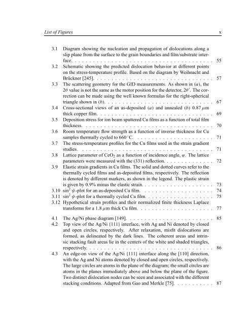
List <strong>of</strong> Figures x<br />
3.1 Diagram show<strong>in</strong>g the nucleation <strong>and</strong> propagation <strong>of</strong> dislocations along a<br />
slip plane from the surface to the gra<strong>in</strong> boundaries <strong>and</strong> film/substrate <strong>in</strong>terface.<br />
...................................... 55<br />
3.2 Schematic show<strong>in</strong>g the predicted dislocation behavior at different po<strong>in</strong>ts<br />
on the stress-temperature pr<strong>of</strong>ile. Based on the diagram by Weihnacht <strong>and</strong><br />
Brückner [245]. . . .............................. 57<br />
3.3 The scatter<strong>in</strong>g geometry for the GID measurements. As shown <strong>in</strong> (a), the<br />
2θ value is not the same as the motor position for the detector, 2θ ′ . The correction<br />
can be made us<strong>in</strong>g the well known formulas for the right-spherical<br />
triangle shown <strong>in</strong> (b). ............................. 67<br />
3.4 Cross-sectional views <strong>of</strong> an as-deposited (a) <strong>and</strong> annealed (b) 0.87 µm<br />
thick copper film................................ 69<br />
3.5 Deposition stress for ion beam sputtered <strong>Cu</strong> films as a function <strong>of</strong> total film<br />
thickness. ................................... 70<br />
3.6 Room temperature flow strength as a function <strong>of</strong> <strong>in</strong>verse thickness for <strong>Cu</strong><br />
samples thermally cycled to 660 ◦ C. ..................... 71<br />
3.7 The stress-temperature pr<strong>of</strong>iles for the <strong>Cu</strong> films used <strong>in</strong> the stra<strong>in</strong> gradient<br />
studies. .................................... 71<br />
3.8 Lattice parameter <strong>of</strong> CeO2 as a function <strong>of</strong> <strong>in</strong>cidence angle, α. The lattice<br />
parameters were measured with the (331) reflection. ............. 72<br />
3.9 Elastic stra<strong>in</strong> gradients <strong>in</strong> <strong>Cu</strong> films. The solid <strong>and</strong> dotted curves refer to the<br />
thermally cycled films <strong>and</strong> as-deposited films, respectively. The reflection<br />
is denoted by different markers, as shown <strong>in</strong> the legend. The plastic stra<strong>in</strong><br />
is given by 0.9% m<strong>in</strong>us the elastic stra<strong>in</strong>. ................... 73<br />
3.10 s<strong>in</strong> 2 ψ-plot for an as-deposited <strong>Cu</strong> film. ................... 74<br />
3.11 s<strong>in</strong> 2 ψ-plot for a thermally cycled <strong>Cu</strong> film................... 75<br />
3.12 Hypothetical stra<strong>in</strong> pr<strong>of</strong>iles <strong>and</strong> their normalized f<strong>in</strong>ite thickness Laplace<br />
transforms for a 1.8 µm thick <strong>Cu</strong> film. .................... 77<br />
4.1 The <strong>Ag</strong>/<strong>Ni</strong> phase diagram [149]. ....................... 85<br />
4.2 Top view <strong>of</strong> the <strong>Ag</strong>/<strong>Ni</strong> {111} <strong>in</strong>terface, with <strong>Ag</strong> <strong>and</strong> <strong>Ni</strong> denoted by closed<br />
<strong>and</strong> open circles, respectively. After relaxation, misfit dislocations are<br />
formed, as del<strong>in</strong>eated by the dark l<strong>in</strong>es. The coherent areas <strong>and</strong> <strong>in</strong>tr<strong>in</strong>sic<br />
stack<strong>in</strong>g fault areas lie <strong>in</strong> the centers <strong>of</strong> the white <strong>and</strong> shaded triangles,<br />
respectively. .................................. 86<br />
4.3 An edge-on view <strong>of</strong> the <strong>Ag</strong>/<strong>Ni</strong> {111} <strong>in</strong>terface along the [110] direction,<br />
with the <strong>Ag</strong> <strong>and</strong> <strong>Ni</strong> atoms denoted by closed <strong>and</strong> open circles, respectively.<br />
The large circles are atoms <strong>in</strong> the plane <strong>of</strong> the diagram; the small circles are<br />
atoms <strong>in</strong> the planes immediately above <strong>and</strong> below the plane <strong>of</strong> the figure.<br />
Two dist<strong>in</strong>ct dislocation nodes can be seen <strong>and</strong> associated with the different<br />
stack<strong>in</strong>g conditions. Adapted from Gao <strong>and</strong> Merkle [75]. . . ........ 87


