Stresses in Cu Thin Films and Ag/Ni Multilayers - Harvard School of ...
Stresses in Cu Thin Films and Ag/Ni Multilayers - Harvard School of ...
Stresses in Cu Thin Films and Ag/Ni Multilayers - Harvard School of ...

You also want an ePaper? Increase the reach of your titles
YUMPU automatically turns print PDFs into web optimized ePapers that Google loves.
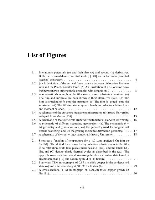
List <strong>of</strong> Figures<br />
1.1 Interatomic potentials (a) <strong>and</strong> their first (b) <strong>and</strong> second (c) derivatives.<br />
Both the Lennard-Jones potential (solid) [140] <strong>and</strong> a harmonic potential<br />
(dashed) are shown. .............................. 4<br />
1.2 (a) A depiction <strong>of</strong> the vertical force balance between dislocation l<strong>in</strong>e tension<br />
<strong>and</strong> the Peach-Koehler force. (b) An illustration <strong>of</strong> a dislocation bow<strong>in</strong>g<br />
between two impenetrable obstacles with separation ℓ. ......... 8<br />
1.3 A schematic show<strong>in</strong>g how the film stress causes substrate curvature. (a)<br />
The film <strong>and</strong> substrate are both shown <strong>in</strong> their stra<strong>in</strong>-free state. (b) The<br />
film is stretched to fit onto the substrate. (c) The film is “glued” onto the<br />
substrate. (d) The film/substrate system bends <strong>in</strong> order to achieve force<br />
<strong>and</strong> moment balance. ............................. 12<br />
1.4 A schematic <strong>of</strong> the curvature measurement apparatus at <strong>Harvard</strong> University.<br />
Adapted from Mull<strong>in</strong> [158]. ......................... 13<br />
1.5 A schematic <strong>of</strong> the four-circle Huber diffractometer at <strong>Harvard</strong> University. . 16<br />
1.6 A schematic <strong>of</strong> different scatter<strong>in</strong>g geometries. (a) The symmetric θ −<br />
2θ geometry <strong>and</strong> χ rotation axis, (b) the geometry used for longitud<strong>in</strong>al<br />
diffuse scatter<strong>in</strong>g, <strong>and</strong> (c) the graz<strong>in</strong>g <strong>in</strong>cidence diffraction geometry. . . . 17<br />
1.7 A schematic <strong>of</strong> the sputter<strong>in</strong>g chamber at <strong>Harvard</strong> University. ........ 18<br />
2.1 Stress as a function <strong>of</strong> temperature for a 1.91 µm sputtered <strong>Cu</strong> film on<br />
Si(100). The dotted l<strong>in</strong>es show the hypothetical elastic stress <strong>in</strong> the film<br />
if no relaxation could take place (thermoelastic l<strong>in</strong>es), <strong>and</strong> the labels (A),<br />
(B), <strong>and</strong> (C) denote elastic thermal cycles as described <strong>in</strong> the text. The<br />
upper thermoelastic l<strong>in</strong>e was drawn us<strong>in</strong>g the elastic constant data found <strong>in</strong><br />
Bechmann et al. [12] <strong>and</strong> assum<strong>in</strong>g mild 〈111〉 texture. . . . ........ 21<br />
2.2 Plan-view TEM micrographs <strong>of</strong> 0.87 µm thick copper <strong>in</strong> the as-deposited<br />
state (a) <strong>and</strong> after anneal<strong>in</strong>g at 600 ◦ C for 0.5 hrs (b). ............ 29<br />
2.3 A cross-sectional TEM micrograph <strong>of</strong> 1.90 µm thick copper grown on<br />
Ge(111). .................................... 30<br />
viii