

Xcell Journal: The authoritative journal for programmable ... - Xilinx
Xcell Journal: The authoritative journal for programmable ... - Xilinx
Xcell Journal: The authoritative journal for programmable ... - Xilinx

You also want an ePaper? Increase the reach of your titles
YUMPU automatically turns print PDFs into web optimized ePapers that Google loves.
ISSUE 51, WINTER 2004 XCELL JOURNAL XILINX, INC.<br />
<strong>Xcell</strong> Issue 51<br />
Winter 2004<br />
<strong>journal</strong><br />
THE AUTHORITATIVE JOURNAL FOR PROGRAMMABLE LOGIC USERS<br />
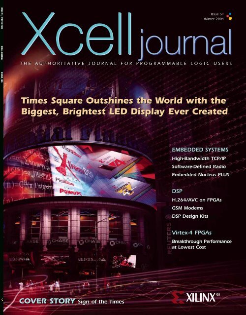
Times Square Outshines the World with the<br />
Biggest, Brightest LED Display Ever Created<br />
COVER STORY Sign of the Times<br />
EMBEDDED SYSTEMS<br />
High-Bandwidth TCP/IP<br />
Software-Defined Radio<br />
Embedded Nucleus PLUS<br />
DSP<br />
H.264/AVC on FPGAs<br />
GSM Modems<br />
DSP HDKs Design <strong>for</strong> DSP Kits Apps<br />
Virtex-4 VIRTEX-4 FPGAs FPGAS<br />
Breakthrough Per<strong>for</strong>mance<br />
at Lowest Cost<br />
R
<strong>The</strong> New SPARTAN <br />
Pb-free devices<br />
available now<br />
Make It<br />
-3<br />
Your ASIC<br />
<strong>The</strong> world’s lowest-cost FPGAs<br />
Spartan-3 Plat<strong>for</strong>m FPGAs deliver everything you need at the price you want. Leading the way in 90nm<br />
process technology, the new Spartan-3 devices are driving down costs in a huge range of high-capability,<br />
cost-sensitive applications. With the industry’s widest density range in its class — 50K to 5 Million<br />
gates — the Spartan-3 family gives you unbeatable value and flexibility.<br />
Lots of features … without compromising on price<br />
Check it out. You get 18x18 embedded multipliers <strong>for</strong> XtremeDSP processing in a low-cost<br />
FPGA. Our unique staggered pad technology delivers a ton of I/Os <strong>for</strong> total connectivity<br />
solutions. Plus our XCITE technology improves signal integrity, while eliminating hundreds<br />
of resistors to simplify board layout and reduce your bill of materials.<br />
With the lowest cost per I/O and lowest cost per logic cell, Spartan-3 Plat<strong>for</strong>m<br />
FPGAs are the perfect fit <strong>for</strong> any design … and any budget.<br />
MAKE IT YOUR ASIC<br />
<strong>The</strong> Programmable Logic Company SM<br />
For more in<strong>for</strong>mation visit<br />
www.xilinx.com/spartan3<br />
©2004 <strong>Xilinx</strong>, Inc., 2100 Logic Drive, San Jose, CA 95124. Europe +44-870-7350-600; Japan +81-3-5321-7711; Asia Pacific +852-2-424-5200; <strong>Xilinx</strong> is a registered trademark, Spartan and XtremeDSP are trademarks, and <strong>The</strong> Programmable Logic Company is a service mark of <strong>Xilinx</strong>, Inc.
EDITOR IN CHIEF Carlis Collins<br />
editor@xilinx.com<br />
408-879-4519<br />
MANAGING EDITOR Forrest Couch<br />
<strong>for</strong>rest.couch@xilinx.com<br />
408-879-5270<br />
ASSISTANT MANAGING EDITOR Charmaine Cooper Hussain<br />
XCELL ONLINE EDITOR Tom Pyles<br />
tom.pyles@xilinx.com<br />
720-652-3883<br />
ADVERTISING SALES Dan Teie<br />
1-800-493-5551<br />
ART DIRECTOR Scott Blair<br />
<strong>Xilinx</strong>, Inc.<br />
2100 Logic Drive<br />
San Jose, CA 95124-3400<br />
Phone: 408-559-7778<br />
FAX: 408-879-4780<br />
© 2004 <strong>Xilinx</strong>, Inc. All rights reserved. XILINX,<br />
the <strong>Xilinx</strong> Logo, and otherdesignated brands included<br />
herein are trademarks of <strong>Xilinx</strong>, Inc. PowerPC is a trademark<br />
of IBM, Inc. All other trademarks are the propert y<br />
of their respective owners.<br />
<strong>The</strong> articles, in<strong>for</strong>mation, and other materials included in<br />
this issue are provided solely <strong>for</strong> the convenience of our<br />
readers. <strong>Xilinx</strong> makes no warranties, express, implied,<br />
statutory, or otherwise, and accepts no liability with respect<br />
to any such articles, in<strong>for</strong>mation, or other materials or<br />
their use, and any use thereof is solely at the risk of the<br />
user. Any person or entity using such in<strong>for</strong>mation in any<br />
way releases and waives any claim it might have against<br />
<strong>Xilinx</strong> <strong>for</strong> any loss, damage, or expense caused thereby.<br />
L E T T E R F R O M T H E E D I T O R<br />
And the Number Please...<br />
What does the number 6,759,852 represent? Well, I guess it could represent a lot of different<br />
things. For example, it could be the current population of Chennai, India. It could be the phone<br />
number of Training Academy Ireland (they’re nice folks, but please don’t call them to verify). Or it<br />
could be the student ID number of a computer science major attending the University of<br />
Manitoba, Canada.<br />
Had you chosen any one of these you would have been correct, but you would not have guessed<br />
the answer I was looking <strong>for</strong>.<br />
On July 6, 2004, <strong>Xilinx</strong> ® reached the 1,000th patent landmark. <strong>The</strong> patent, “VDD Detection Path<br />
in Power-Up Circuit,” was U.S. Patent number 6,759,852. (I can’t believe you didn’t guess this.)<br />
It was issued to Maheen A. Samad in our General Products Division, Engineering department.<br />
So what’s the big deal, you might ask? Although our corporate pride may runneth over, our patent<br />
count doesn’t hold a candle to some corporate giants. That may be true, but <strong>Xilinx</strong> was founded<br />
with innovation at its core, beginning with Ross Freeman’s invention of the FPGA and continuing<br />
with innovative practices and ideas, many of which are commemorated in the patent hallway at our<br />
corporate headquarters.<br />
Using our R&D dollars as a metric to measure our efficiency in converting innovation into patents,<br />
<strong>Xilinx</strong> – as a high-tech company – ranks second only to IBM. <strong>Xilinx</strong> also ranks 131st in the<br />
number of patents held, making it one of the most innovative companies worldwide.<br />
This milestone – while not hugely significant in terms of the raw number – is more about<br />
celebrating the continued innovation from <strong>Xilinx</strong>, both in the <strong>for</strong>m of technology patents as well<br />
as business acumen.<br />
This issue of the <strong>Xcell</strong> <strong>Journal</strong> features articles in two key technology areas: digital signal<br />
processing (DSP) and embedded processors. This issue also includes an article on the new Virtex-4<br />
family of FPGAs, which offers three plat<strong>for</strong>ms optimized <strong>for</strong> logic, DSP, and embedded processor<br />
applications. And speaking of innovation, the Virtex-4 family includes more than 120 new (and,<br />
of course, patented) features, many of which are specific to supporting high-per<strong>for</strong>mance signal<br />
processing and embedded processors.<br />
With the launch of the Virtex-4 multi-plat<strong>for</strong>m FPGA family, the <strong>Xilinx</strong> vision expands to encompass<br />
<strong>programmable</strong> systems, which include logic, embedded processing, and very high-per<strong>for</strong>mance digital<br />
signal processing. As illustrated in the many articles in this issue, <strong>programmable</strong> technologies provide<br />
customers further flexibility and per<strong>for</strong>mance benefits to inspire innovation.<br />
Forrest Couch<br />
Managing Editor
9<br />
Embedded with <strong>Xilinx</strong><br />
In this series on embedded processing,<br />
the <strong>Xcell</strong> <strong>Journal</strong> samples a broad base<br />
of embedded processing applications.<br />
COVER STORY<br />
Sign of the Times<br />
<strong>Xilinx</strong> makes high-tech<br />
outdoor advertising in<br />
Times Square possible.<br />
10<br />
T A B L E O F C O N T E N T S<br />
EMBEDDED SYSTEMS DIGITAL SIGNAL PROCESSING<br />
39<br />
Taking Digital Signal<br />
Processing to the Extreme<br />
In this series on digital signal processing,<br />
the <strong>Xcell</strong> <strong>Journal</strong> spotlights the challenges<br />
of and solutions to developing extremely<br />
high-per<strong>for</strong>mance DSP applications.
W I N T E R 2 0 0 4, I S S U E 5 1<br />
Considerations <strong>for</strong><br />
High-Bandwidth<br />
TCP/IP PowerPC<br />
Applications<br />
<strong>The</strong> <strong>Xilinx</strong> Gigabit System<br />
Reference Design maximizes<br />
TCP/IP per<strong>for</strong>mance. 14<br />
Virtex-4:<br />
Breakthrough<br />
Per<strong>for</strong>mance at<br />
the Lowest Cost<br />
Virtex-4 FPGAs deliver what<br />
you’ve been looking <strong>for</strong>.<br />
33<br />
Implementing the<br />
H.264/AVC Video<br />
Coding Standard<br />
on FPGAs<br />
<strong>Xilinx</strong> Virtex FPGAs provide<br />
excellent co-, pre-, and<br />
post-processing hardware<br />
acceleration solutions.<br />
Simulink Brings<br />
Model-Based Design<br />
to Embedded<br />
Signal Processing<br />
40<br />
<strong>The</strong> complexity of FPGA-based<br />
signal processing systems<br />
drives the need <strong>for</strong> new<br />
development approaches.66<br />
<strong>Xcell</strong> <strong>Xcell</strong><strong>journal</strong> <strong>journal</strong><br />
View from the Top ................................................................6<br />
Embedded with <strong>Xilinx</strong>............................................................9<br />
Sign of the Times ...............................................................10<br />
High-Bandwidth TCP/IP PowerPC Applications.........................14<br />
Embedded Nucleus PLUS RTOS Using <strong>Xilinx</strong> EDK .....................17<br />
MicroBlaze and PowerPC as Test Generators...........................20<br />
Nohau Shortens Embedded Processor Debug Time...................23<br />
Scalable Software-Defined Radio Development........................26<br />
High-Speed Optical Burst Switching .......................................29<br />
Virtex-4: Breakthrough Per<strong>for</strong>mance/Lowest Cost ...................33<br />
Taking DSP to the Extreme ..................................................39<br />
Implementing H.264/AVC Video Coding Standard ..................40<br />
GSM Modem on a DSP/FPGA Architecture .............................44<br />
Design Kits Turbo-Charge DSP Applications..............................48<br />
System Generator to Create J.83 Cable Modulator ..................51<br />
Implementing DSP Algorithms in FPGAs .................................56<br />
XtremeDSP Slices Deliver More GMACs ..................................60<br />
Image Processing Algorithms with System Generator ...............63<br />
Simulink <strong>for</strong> Embedded Signal Processing...............................66<br />
Interfacing Simulink to the Analog World ...............................70<br />
Build Custom Real-Time Video Applications .............................74<br />
Let System Generator Do the Handshaking.............................78<br />
Early Access: <strong>The</strong> Designer’s Edge .........................................81<br />
70 High-Speed Channels with 9 FPGAs..................................89<br />
LIN Bus – Cost-Effective Alternative to CAN ............................92<br />
Education Services Trims Learning Curve ................................96<br />
Board of Education .............................................................99<br />
Flexible and Adaptable IP Interconnection.............................101<br />
Simplify FPGA Application Design with DIMEtalk....................104<br />
Design Once <strong>for</strong> ASIC Prototypes.........................................108<br />
To subscribe to the <strong>Xcell</strong> <strong>Journal</strong><br />
or to view the web-based <strong>Xcell</strong> Online,<br />
visit www.xilinx.com/xcell/.
View<br />
from the top<br />
Focusing on<br />
Programmable<br />
Technologies<br />
<strong>Xilinx</strong> clearly leads the <strong>programmable</strong> logic<br />
business; now we are expanding into<br />
other key <strong>programmable</strong> technologies.<br />
by Wim Roelandts<br />
CEO, <strong>Xilinx</strong>, Inc.<br />
Throughout the<br />
history of semiconductors,<br />
when a<br />
technology becomes<br />
<strong>programmable</strong>, it<br />
dominates. That’s<br />
why, in addition to<br />
<strong>programmable</strong><br />
logic, we have<br />
defined two key<br />
<strong>programmable</strong><br />
technologies on which we will focus: digital<br />
signal processing and embedded processing.<br />
We have the right technology and the right<br />
business model to be a major player in all of<br />
these important and fast-growing markets.<br />
Digital Signal Processing<br />
<strong>Xilinx</strong> FPGAs have long been the highest<br />
per<strong>for</strong>mance technology <strong>for</strong> building DSP<br />
designs. With our devices and software,<br />
you can build systems that are two to three<br />
orders of magnitude faster than what a dedicated<br />
DSP device can do on its own.<br />
Putting our extremely high per<strong>for</strong>mance<br />
DSP functionality next to a <strong>programmable</strong><br />
DSP allows DSP designers to develop systems<br />
with unprecedented per<strong>for</strong>mance and<br />
value. You also get many other advantages<br />
offered by FPGAs, including flexibility, fast<br />
time to market, and higher levels of system<br />
integration. <strong>The</strong>re simply is no easier,<br />
faster, or better way to develop extreme<br />
per<strong>for</strong>mance DSP designs.<br />
For example, with our new Virtex-4<br />
FPGA family, you can achieve 256<br />
GigaMACs (billions of multiple accumulates<br />
per second). We have achieved this<br />
amazing per<strong>for</strong>mance through both<br />
advanced architecture and silicon fabrication<br />
technologies.<br />
Applications <strong>for</strong> our high-per<strong>for</strong>mance<br />
DSP capabilities are growing. Broadcasting<br />
or video conferencing <strong>for</strong> high-definition<br />
television, <strong>for</strong> example, is rapidly being<br />
converted to the H.264 <strong>for</strong>mat. This standard<br />
requires a lot of processing power, as<br />
the target is to have the quality of MPEG-<br />
2 video at one-half the bit rate.<br />
Sophisticated motion compensation<br />
schemes are being used to achieve this goal.<br />
Standard video processors can per<strong>for</strong>m this<br />
6 <strong>Xcell</strong> <strong>Journal</strong> Winter 2004
function at smaller screen sizes up to common<br />
intermediate <strong>for</strong>mat (CIF) resolutions,<br />
but to go beyond this to standard<br />
definition (SD) or high definition (HD)<br />
requires the per<strong>for</strong>mance of a <strong>Xilinx</strong> FPGA<br />
to per<strong>for</strong>m some of the more math-intensive<br />
functions (such as motion estimation)<br />
in conjunction with a <strong>programmable</strong> video<br />
processor. Our DSP capability makes<br />
<strong>Xilinx</strong> the technology of choice <strong>for</strong> these<br />
new demanding applications.<br />
For years the only other solution <strong>for</strong> these<br />
very high per<strong>for</strong>mance DSP applications<br />
was custom devices – ASICs. Yet ASICs take<br />
far longer to design, cost much more to<br />
develop, cannot easily be modified to meet<br />
changing requirements, and are risky because<br />
of their complexity. <strong>Xilinx</strong> <strong>programmable</strong><br />
devices and development tools provide a far<br />
better solution with less overall cost.<br />
Today, the high-per<strong>for</strong>mance FPGAbased<br />
DSP market alone is worth more<br />
than $200 million, and we have over 80%<br />
of that market. According to market estimates,<br />
the DSP market addressable by<br />
FPGAs is expected to grow to more than<br />
$3 billion by 2007. So, as you can see, the<br />
future looks very bright <strong>for</strong> <strong>Xilinx</strong> as the<br />
demand <strong>for</strong> very high per<strong>for</strong>mance DSP<br />
continues to grow. We are well positioned<br />
to provide the devices, the development<br />
tools, and the support services to meet this<br />
growing demand.<br />
Embedded Processing<br />
We are relatively new to the embedded processing<br />
market – three years ago we introduced<br />
our Virtex-II Pro family, which<br />
includes an embedded hard-core IBM<br />
PowerPC processor. Although it took<br />
awhile <strong>for</strong> the idea to catch on, we now have<br />
thousands of design wins using our embedded<br />
processors. And in addition to the<br />
PowerPC processor, we now offer our 32-bit<br />
MicroBlaze and the 8-bit PicoBlaze<br />
soft-core processors. All of these embedded<br />
processors work together, using the same<br />
peripherals and IP, so you can easily create<br />
complete high-per<strong>for</strong>mance, multi-processor<br />
systems on a single low-cost chip.<br />
<strong>The</strong> total embedded processor market is<br />
very fragmented because there are multiple<br />
architectures and multiple operating sys-<br />
V I E W F R O M T H E T O P<br />
tems. Customers tend to stay with a known<br />
architecture because of their long-term software<br />
investment – no one wants to re-code<br />
and re-port their designs to a new architecture.<br />
That’s one reason why we chose the<br />
PowerPC as our high-per<strong>for</strong>mance processor,<br />
because (except <strong>for</strong> cell phones and<br />
video games) it is the one most used in our<br />
industry, and it is well supported by both<br />
IBM and Motorola. Capturing even a relatively<br />
small percentage of this $15 billion<br />
market would mean significant revenue <strong>for</strong><br />
<strong>Xilinx</strong>. Many embedded processing customers<br />
are beginning to realize the benefits<br />
of our technology – and we’ve only started<br />
to focus on this market segment.<br />
Because our MicroBlaze and PicoBlaze<br />
processors are created as soft cores, they are<br />
very flexible and extensible. Plus, they are<br />
fast enough to meet the needs of many<br />
applications, very inexpensively. Combined<br />
with our high-per<strong>for</strong>mance PowerPC<br />
processor, they <strong>for</strong>m an unbeatable alliance<br />
that can handle the most demanding applications<br />
with ease, all on a single <strong>programmable</strong><br />
device.<br />
Our processor strategy is to provide a<br />
range of embedded processors, all using<br />
the same peripherals and IP, all working<br />
together seamlessly on a single chip, and<br />
working seamlessly with our DSP and<br />
logic functions. Thus you can build and<br />
simulate very complex systems and produce<br />
production-ready designs faster than<br />
ever be<strong>for</strong>e. <strong>The</strong>n, as your requirements<br />
change or as design errors are uncovered,<br />
you can quickly modify your design and<br />
resume production without losing customers.<br />
That’s the power of programmability;<br />
that’s what <strong>Xilinx</strong> does best. <strong>The</strong><br />
advantages are enormous.<br />
Focusing on the Future<br />
Our original focus was on supporting logic<br />
designers – the traditional customers <strong>for</strong> our<br />
devices. However, DSP and embedded processing<br />
designers are very different from logic<br />
designers; they use different tools, they have<br />
different needs and expectations, and they<br />
approach their designs in different ways. For<br />
example, DSP designers usually work with<br />
algorithms such as Fast Fourier Trans<strong>for</strong>ms<br />
and FIR filters; embedded processing design-<br />
ers work with high-level languages such as C<br />
or C++, while logic designers usually work in<br />
VHDL or Verilog. Although the final<br />
implementation is in an FPGA, the design<br />
approach is very different <strong>for</strong> each of these<br />
customers, and thus we must support these<br />
customers in different ways.<br />
<strong>The</strong>re<strong>for</strong>e, to ensure that we are addressing<br />
the needs of each market segment, I<br />
decided to create two new divisions within<br />
<strong>Xilinx</strong>; one to focus on the DSP market<br />
and one to focus on the embedded processing<br />
market. Each new division, headed by a<br />
vice president, will focus on providing the<br />
development tools, devices, IP (cores), support<br />
services, and marketing functions to<br />
fully capitalize on these growing technologies.<br />
We intend to be the leader in all of<br />
these key <strong>programmable</strong> technologies.<br />
Conclusion<br />
<strong>Xilinx</strong> is the only company that can bring<br />
all these <strong>programmable</strong> technologies<br />
together in a single device, giving you a<br />
tremendous advantage in per<strong>for</strong>mance,<br />
cost, and time to market. If you do a system-on-chip<br />
design in an ASIC, it will<br />
require tens of millions of dollars in upfront<br />
(NRE) investment, and ASIC designs<br />
are risky because you not only have to do<br />
the logic design – you must also do the<br />
physical design. This can only be justified<br />
<strong>for</strong> high-volume, low-cost applications.<br />
With <strong>Xilinx</strong> you can do a system-onchip<br />
design with no NRE. And because the<br />
chip itself is already designed and<br />
debugged, you don’t need to worry about<br />
physical design issues such as crosstalk and<br />
power distribution. All you need to do is<br />
develop the logic design, which can be<br />
quick and easy using our growing family of<br />
IP and development tools that solve many<br />
complex design problems <strong>for</strong> you.<br />
Basically, now we can offer a systemon-chip<br />
<strong>for</strong> the masses, because now we<br />
have the advantages of an ASIC in a flexible<br />
and <strong>programmable</strong> device. Now you<br />
can create a single chip that includes DSP<br />
and embedded processors, along with IP<br />
and custom logic, <strong>for</strong> much less cost and<br />
no risk. All these <strong>programmable</strong> technologies,<br />
available on a single device, give you<br />
a significant advantage.<br />
Winter 2004 <strong>Xcell</strong> <strong>Journal</strong> 7
Embedded with <strong>Xilinx</strong><br />
In this series on embedded processing, the <strong>Xcell</strong> <strong>Xcell</strong> <strong>Journal</strong> <strong>Journal</strong><br />
samples a broad base of embedded processing applications.<br />
by Mark Aaldering<br />
Vice President, Embedded Processing Division<br />
<strong>Xilinx</strong>, Inc.<br />
mark.aaldering@xilinx.com<br />
In today’s world, just about every system incorporates some <strong>for</strong>m of embedded processing<br />
in an amazing array of markets and applications. During the last few years,<br />
<strong>Xilinx</strong>, our partners, and our customers have developed and shared a vision to build<br />
and assemble all of the elements required <strong>for</strong> a complete and robust range of embedded<br />
processing solutions adapted <strong>for</strong> FPGA technologies.<br />
In this edition of the <strong>Xcell</strong> <strong>Journal</strong>, we have assembled articles representing a wide<br />
range of embedded processing applications. <strong>The</strong>se include articles on state-of-the-art<br />
commercial applications, real-time operating systems, multi-processor debugging environments,<br />
testing of complex hardware modules, and high-speed Internet communication<br />
protocols.<br />
With our accelerated success in the embedded processing arena, it is appropriate<br />
that this series of articles coincides with the recently announced <strong>for</strong>mation of the<br />
Embedded Processing Division. This division brings talent and technology together in<br />
an organization to accelerate development of an even wider range of embedded system<br />
solutions, optimizing the full capabilities of our silicon architectures at multiple per<strong>for</strong>mance<br />
and price points.<br />
This new division rein<strong>for</strong>ces our commitment to the increasingly diverse and<br />
changing embedded systems market and represents the evolution of three years of<br />
embedded processing experience.<br />
EMBEDDED SYSTEMS<br />
Table of Contents<br />
Sign of the Times ....................................10<br />
High-Bandwidth TCP/IP<br />
PowerPC Applications ...............................14<br />
Embedded Nucleus PLUS RTOS<br />
Using <strong>Xilinx</strong> EDK......................................17<br />
MicroBlaze and PowerPC<br />
as Test Generators ...................................20<br />
Nohau Shortens Embedded<br />
Processor Debug Time ..............................23<br />
Scalable Software-Defined<br />
Radio Development..................................26<br />
High-Speed Optical Burst Switching ............29<br />
Winter 2004 <strong>Xcell</strong> <strong>Journal</strong> 9
EMBEDDED SYSTEMS<br />
Sign of the Times<br />
<strong>Xilinx</strong> makes high-tech outdoor advertising in Times Square possible.<br />
by Jason Daughenbaugh<br />
Sr. Design Engineer<br />
Advanced Electronic Designs, Inc.<br />
jason.daughenbaugh@aedmt.com<br />
New York City’s Times Square is known<br />
as the “Crossroads of the World.”<br />
Approximately 1.5 million people pass<br />
through the intersection of Broadway and<br />
42nd Street every day, and millions more<br />
see the area daily on television broadcasts.<br />
No better place <strong>for</strong> outdoor advertising<br />
exists. As a result, dazzling signs have<br />
become a Times Square trademark.<br />
Every advertiser wants to have the best<br />
advertising medium possible, so new signs<br />
must use the latest technology. Times<br />
Square tenants rely on MultiMedia, which<br />
manufactures the majority of the spectacular<br />
signs in Times Square. When<br />
MultiMedia asked our company, Advanced<br />
Electronic Designs, Inc. (AED), to design an<br />
LED sign <strong>for</strong> JPMorgan Chase in Times<br />
Square, we needed a huge amount of signal<br />
processing, data distribution, and interfacing.<br />
We also needed to design the sign very<br />
quickly. We met this challenge by utilizing<br />
the advantages of <strong>Xilinx</strong> ® components.<br />
We used Virtex-II XC2V1000 FPGAs<br />
<strong>for</strong> video processing, and <strong>for</strong> control and<br />
distribution we chose low-cost Spartan-3<br />
XC3S200 FPGAs. To configure the FPGAs,<br />
we chose the Plat<strong>for</strong>m Flash XCF00 configuration<br />
PROM family. And <strong>for</strong> final distribution<br />
of the data on the 3800 LED blocks,<br />
we used XC9572XL PLDs.<br />
10 <strong>Xcell</strong> <strong>Journal</strong> Winter 2004
<strong>The</strong> Design<br />
An LED sign is like a large computer monitor;<br />
video data goes in and is displayed on<br />
the sign. <strong>The</strong> sign comprises red, green,<br />
and blue LEDs that turn on and off (pulsewidth<br />
modulation) to generate more than<br />
four trillion colors.<br />
What made this particular design a<br />
challenge was the scale, both in terms of<br />
physical size as well as the amount of data<br />
and the transfer rates involved. <strong>The</strong> sign is<br />
135 feet long and 26 feet tall. With nearly<br />
two million pixels, it is the highest definition<br />
LED display in the world. This is ten<br />
times the resolution of the average television<br />
screen and twice the resolution of topof-the-line<br />
HDTV sets.<br />
After considering our options, designing<br />
with <strong>Xilinx</strong> <strong>programmable</strong> logic was<br />
the obvious choice. <strong>The</strong> high-per<strong>for</strong>mance,<br />
low-cost FPGAs are well suited <strong>for</strong><br />
all three main components of this design:<br />
video processing, data distribution, and<br />
sign control.<br />
Video Processing<br />
<strong>The</strong> video processor accepts a variety of<br />
video inputs. It captures these video streams<br />
as 36 bit RGB (12 bits per color). It then<br />
crops and places these inputs onto a master<br />
sign image <strong>for</strong> display. Color-space conversion<br />
adjusts image characteristics such as<br />
color temperature and balance.<br />
Additional processing corrects<br />
<strong>for</strong> individual LED<br />
differences. We also use proprietary<br />
image processing<br />
algorithms to operate the<br />
LEDs efficiently while maintaining<br />
optimal image quality.<br />
Data Distribution<br />
Video data starts in a control<br />
room and ends at the LEDs. <strong>The</strong><br />
first step is the video processor,<br />
which is located in the control<br />
room. <strong>The</strong> video processor breaks the<br />
images into manageable chunks to send to<br />
the many modules of the sign so that each<br />
LED displays the data <strong>for</strong> the corresponding<br />
pixel. More than 3 Gbps of video data<br />
alone is required to operate the LEDs. In<br />
addition to video data, we also transfer a<br />
Figure 1 – <strong>The</strong> world’s highest resolution LED display is based on <strong>Xilinx</strong> devices.<br />
Figure 2 – <strong>The</strong> sign is built<br />
out of 3,800 display blocks.<br />
variety of control and status functions.<br />
Not wanting to re-invent the wheel,<br />
we chose Ethernet as our data distribution<br />
medium. Our video processor has<br />
multiple Gigabit Ethernet ports that<br />
interface to the sign. Gigabit Ethernet<br />
can be transferred over fiber-optic cable,<br />
EMBEDDED SYSTEMS<br />
allowing great distances between the controller<br />
and the sign itself.<br />
We were able to use off-the-shelf switches<br />
to distribute the data within the sign and put<br />
inexpensive 10/100 Ethernet ports on the<br />
individual distribution boards. <strong>The</strong> availability<br />
of Ethernet protocol analyzers,<br />
such as the open-source project<br />
Ethereal, allowed us to easily analyze<br />
and debug the system.<br />
Sign Control<br />
In advertising, time is money; thus it is crucial<br />
to monitor the sign at all times. <strong>The</strong><br />
control system monitors temperatures<br />
throughout the sign to ensure that adequate<br />
cooling is present. Voltages are monitored to<br />
detect malfunctioning power supplies. <strong>The</strong><br />
control system maintains error and resend<br />
counts to detect faulty data links. It also provides<br />
an interface to upgrade the FPGAs<br />
remotely <strong>for</strong> enhancements and bug fixes.<br />
Winter 2004 <strong>Xcell</strong> <strong>Journal</strong> 11
EMBEDDED SYSTEMS<br />
<strong>The</strong> reconfigurable nature of <strong>Xilinx</strong> FPGAs allows us to provide<br />
feature upgrades and bug fixes to the customer via e-mail...<br />
<strong>The</strong> Benefits of <strong>Xilinx</strong> Devices<br />
<strong>Xilinx</strong> devices include a large number of<br />
features that are ideal <strong>for</strong> our sign project:<br />
• <strong>The</strong> reconfigurable nature of <strong>Xilinx</strong><br />
devices is necessary <strong>for</strong> a project like<br />
this. Without FPGAs, the only alternative<br />
would have been an ASIC. But an<br />
ASIC was not feasible <strong>for</strong> this project<br />
<strong>for</strong> several reasons.<br />
First, this project had a very tight schedule.<br />
An ASIC could not have been completed<br />
in the time allotted. Second, the<br />
volumes of the components in this sign<br />
are not of sufficient volume to hide the<br />
NREs of an ASIC. Third, an ASIC lacks<br />
the development opportunities of an<br />
FPGA. To me, as an engineer, this reason<br />
is the most important. No matter<br />
how much simulation you per<strong>for</strong>m,<br />
there can always be unexpected bugs. In<br />
an ASIC, these bugs are expensive; in an<br />
FPGA, they can be fixed easily.<br />
Another FPGA advantage is that it can<br />
meet future needs through feature<br />
upgrades; an ASIC cannot. <strong>The</strong> reconfigurable<br />
nature of <strong>Xilinx</strong> FPGAs<br />
allows us to provide feature upgrades<br />
and bug fixes to the customer via email,<br />
making it easy <strong>for</strong> them to apply<br />
to the sign. Through an Ethernet interface,<br />
the FPGA reprograms the<br />
Plat<strong>for</strong>m Flash configuration PROM<br />
and automatically reboots.<br />
• Video processing requires a large number<br />
of multiply operations. <strong>The</strong> video<br />
processor must per<strong>for</strong>m color-space<br />
conversion and apply calibration coefficients<br />
in real time. It would require a<br />
large portion of FPGA logic resources to<br />
build multipliers. Instead, this can be<br />
done very efficiently by utilizing the<br />
embedded multipliers. Building<br />
pipelined processing structures with the<br />
embedded multipliers allowed us to easily<br />
meet the processing requirements.<br />
• This design required a large variety of<br />
signaling standards. <strong>The</strong> flexible <strong>Xilinx</strong><br />
I/O blocks allowed us to connect directly<br />
to a large number of different interfaces.<br />
Voltages ranged from standard<br />
3.3V CMOS down to 1.5V HSTL.<br />
We required single-ended and differential<br />
interfaces. In some cases we could<br />
have used external driver and receiver<br />
parts, but that would have added complexity<br />
and cost to the product.<br />
Other high-speed I/O interfaces, such<br />
as to the DDR 333 memory, would not<br />
have been possible without direct<br />
FPGA support. <strong>The</strong> digitally controlled<br />
impedance (DCI) modes were necessary<br />
on the high-speed single-ended traces.<br />
• With the high data rates involved and<br />
the many data interfaces, we had a large<br />
number of clock domains. <strong>The</strong> quantity<br />
of global clock nets available and the<br />
ability of the digital clock managers<br />
(DCMs) to synthesize clock frequencies<br />
made this easy. We also used the phaseshift<br />
ability of the DCM to adjust sample<br />
times on various interfaces.<br />
• Block RAM is my favorite resource in<br />
an FPGA. Without block RAM, there<br />
are two memory options. <strong>The</strong> first<br />
option is the logic slices, using flipflops<br />
or distributed RAM, but this is<br />
expensive and slow <strong>for</strong> anything more<br />
than 16- to 32-bit addresses. <strong>The</strong> second<br />
option is external memory, such<br />
as SDRAM. SDRAM storage is generally<br />
in the range of tens to hundreds of<br />
megabytes, leaving a huge size gap<br />
between these two memory options.<br />
Block RAM bridges this size gap. It can<br />
be used <strong>for</strong> a limitless number of<br />
things, from FIFOs <strong>for</strong> processing<br />
engines to loadable tables <strong>for</strong> data conversions.<br />
<strong>The</strong> flexible port-widths of<br />
block RAM allow you to use them<br />
individually or in efficient combinations.<br />
<strong>The</strong> dual-port capability makes<br />
them easy to use <strong>for</strong> transferring data<br />
between clock domains or sharing data.<br />
• While very powerful and convenient,<br />
the PLDs and Spartan-3 FPGAs are<br />
also very inexpensive. When combined<br />
with the development advantages, the<br />
low device price makes <strong>Xilinx</strong> devices<br />
unbeatable when developing high-per<strong>for</strong>mance<br />
embedded systems.<br />
PicoBlaze Processors<br />
Device hardware capabilities are essential<br />
<strong>for</strong> any design, but development tools and<br />
tricks are also very important. <strong>The</strong> favorite<br />
toy in our <strong>Xilinx</strong> bag-of-tricks is the<br />
PicoBlaze processor. We could not have<br />
completed the project in the time allowed<br />
without extensive use of the PicoBlaze<br />
processor. <strong>The</strong> sign contains an impressive<br />
count of more than 1,000 of these embedded<br />
processors, with nine different designs.<br />
PicoBlaze processors provide efficient<br />
logic resource utilization by time-multiplexing<br />
logic circuits. Many functions, especially<br />
control functions, do not need to be<br />
10 XC2V1000 Virtex-II FPGA<br />
323 XC3S200 Spartan-3 FPGA<br />
333 XCF00 Plat<strong>for</strong>m Flash PROM<br />
3,800 XC9572XL 72 macrocell PLD<br />
Table 1 – This sign includes nearly<br />
4,500 <strong>Xilinx</strong> devices.<br />
8 Gbps video processing<br />
18 Billion 16-bit multiply<br />
operations per second<br />
16 DDR333 SDRAM banks<br />
6 Gigabit Ethernet MACs<br />
333 Fast Ethernet MACs<br />
>1000 PicoBlaze Processors<br />
Table 2 – <strong>Xilinx</strong> devices achieve<br />
impressive specifications.<br />
12 <strong>Xcell</strong> <strong>Journal</strong> Winter 2004
especially fast, or don’t happen very often.<br />
One example of this would be a serial<br />
transfer to read a temperature sensor. For<br />
this application, the sensor only needs to<br />
be read every ten seconds. It would be a<br />
waste to have a state machine <strong>for</strong> temperature<br />
sensor reading that ran once every ten<br />
seconds but only took a few milliseconds<br />
to complete. <strong>The</strong> logic would be unused<br />
99.9% of the time.<br />
<strong>The</strong>se types of functions can be efficiently<br />
combined into a single PicoBlaze<br />
processor, which in the previous example<br />
can not only read the temperature every ten<br />
seconds but per<strong>for</strong>m other similar tasks in<br />
the meantime.<br />
<strong>The</strong> PicoBlaze processor also provides a<br />
quick and easy way to develop control<br />
functions. <strong>The</strong> alternative would be to<br />
build a custom state machine <strong>for</strong> each<br />
function. <strong>The</strong> PicoBlaze processor is a <strong>programmable</strong><br />
state machine, meaning that<br />
the state machine is already built; one just<br />
has to program it. It has an intuitive and<br />
powerful instruction set and a large codespace<br />
of 1,024 instructions. Programming<br />
the PicoBlaze processor is a quick and easy<br />
way to define many functions.<br />
<strong>The</strong> PicoBlaze processor is also a great<br />
tool <strong>for</strong> accelerating the testing and debugging<br />
process. <strong>The</strong> PicoBlaze program code<br />
is stored in block RAM. To make a change<br />
to the program we only need to change the<br />
block RAM contents. It is possible to do<br />
this without re-implementing the FPGA,<br />
saving a lot of time.<br />
Our favorite method of PicoBlaze<br />
processor development, which is slightly<br />
unique, is to use a PC serial port and a sim-<br />
Figure 3 – <strong>The</strong> video data distribution board is based on an XC3S200 FPGA. It also includes SRAM,<br />
a 10/100 Ethernet port, a status display, and numerous connections to display blocks.<br />
ple PC application to download the program<br />
code into the block RAM of a<br />
configured FPGA. We have developed an<br />
interface board that connects to the FPGA<br />
and has the serial port, as well as several<br />
seven-segment displays to which the<br />
PicoBlaze processor can write <strong>for</strong> debugging.<br />
We also allow the selection of different<br />
processors so that we can work on multiple<br />
processors through the same interface.<br />
This interface is not only useful <strong>for</strong><br />
debugging PicoBlaze programs, but also<br />
<strong>for</strong> debugging the logic connected to the<br />
EMBEDDED SYSTEMS<br />
processor. Because it is so quick and easy<br />
to write programs <strong>for</strong> PicoBlaze processors,<br />
it is very straight<strong>for</strong>ward to write<br />
programs to test the various logic circuits<br />
attached to the processor. We can test each<br />
function individually, greatly simplifying<br />
and accelerating any debugging that<br />
becomes necessary.<br />
A key application of the PicoBlaze<br />
processor in this project is the Ethernet<br />
controller. As mentioned earlier, we selected<br />
Ethernet to distribute data throughout<br />
the sign. At each Ethernet connection, we<br />
have an Ethernet physical layer transceiver<br />
(PHY) device connected directly to an<br />
FPGA. We developed a very simple and<br />
tiny media access controller (MAC) module,<br />
which we use inside the FPGA to connect<br />
the PHY to an instantiation of the<br />
PicoBlaze processor.<br />
This Ethernet unit is small, requiring<br />
less than a quarter of the logic resources<br />
in the XC3S200 FPGA. It handles the<br />
basic Ethernet layers and protocols,<br />
including ARP (address resolution protocol).<br />
It also supports the IP (Internet<br />
protocol) layer with ICMP (Internet<br />
control message protocol), UDP (user<br />
datagram protocol), and DHCP (dynamic<br />
host configuration protocol). With<br />
this Ethernet controller, we can plug an<br />
FPGA into our network and it negotiates<br />
an IP address. <strong>The</strong>n we can transfer files<br />
and data to and from it.<br />
Conclusion<br />
<strong>Xilinx</strong> devices made the challenge of developing<br />
the world’s highest definition LED<br />
display achievable. <strong>The</strong>se devices are a perfect<br />
fit <strong>for</strong> a complex design because of<br />
their flexible nature and powerful feature<br />
set. Valuable design components such as<br />
the PicoBlaze processor further increase<br />
their ease of use and thus their value.<br />
<strong>The</strong> reconfigurable and flexible nature<br />
of the devices allowed us to ship the sign<br />
with all first-revision circuit boards,<br />
enabling us to develop a very complex system<br />
in very little time.<br />
For more in<strong>for</strong>mation about MultiMedia<br />
LED signs, visit www.multimediaLED.com.<br />
For more in<strong>for</strong>mation about the engineering<br />
provided by AED, visit www.aedmt.com.<br />
Winter 2004 <strong>Xcell</strong> <strong>Journal</strong> 13
EMBEDDED SYSTEMS<br />
Considerations <strong>for</strong> High-Bandwidth<br />
TCP/IP PowerPC Applications<br />
<strong>The</strong> <strong>Xilinx</strong> Gigabit System Reference Design<br />
maximizes TCP/IP per<strong>for</strong>mance.<br />
by Chris Borrelli<br />
Embedded Networking Manager<br />
<strong>Xilinx</strong>, Inc.<br />
chris.borrelli@xilinx.com<br />
<strong>The</strong> TCP/IP protocol suite is the de facto<br />
worldwide standard <strong>for</strong> communications<br />
over the Internet and almost all intranets.<br />
Interconnecting embedded devices is<br />
becoming standard practice even in device<br />
classes that were previously stand-alone<br />
entities.<br />
By its very definition, an embedded architecture<br />
has constrained resources, which is<br />
often at odds with rising application requirements.<br />
Achieving wire-speed TCP/IP per<strong>for</strong>mance<br />
continues to be a significant<br />
engineering challenge, even <strong>for</strong> high-powered<br />
Intel Pentium-class PCs.<br />
In this article, we’ll discusses the per-byte<br />
and per-packet overheads limiting TCP/IP<br />
per<strong>for</strong>mance and present the techniques utilized<br />
in the <strong>Xilinx</strong> Gigabit System Reference<br />
Design (GSRD) to maximize TCP/IP over<br />
Gigabit Ethernet per<strong>for</strong>mance in embedded<br />
PowerPC-based applications.<br />
14 <strong>Xcell</strong> <strong>Journal</strong> Winter 2004
GSRD Overview<br />
<strong>The</strong> GSRD terminates IP-based transport protocols<br />
such as TCP or UDP. It incorporates the<br />
embedded PowerPC and RocketIO blocks<br />
of the Virtex-II Pro device family, and is<br />
delivered as an Embedded Development Kit<br />
(EDK) reference system.<br />
<strong>The</strong> reference system as described in<br />
<strong>Xilinx</strong> Application Note XAPP536 leverages<br />
a multi-port DDR SDRAM memory<br />
controller to allocate memory bandwidth<br />
between the PowerPC processor local bus<br />
(PLB) interfaces and two data ports. Each<br />
data port is attached to a direct memory<br />
access (DMA) controller, allowing hardware<br />
peripherals high-bandwidth access to<br />
memory.<br />
A MontaVista Linux port is available<br />
<strong>for</strong> applications requiring an embedded operating<br />
system, while a commercial standalone<br />
TCP/IP stack from Treck is also available to<br />
satisfy applications with the highest bandwidth<br />
requirements.<br />
System Architecture<br />
Memory bandwidth is an important consideration<br />
<strong>for</strong> high-per<strong>for</strong>mance networkattached<br />
applications. Typically, external<br />
DDR memory is shared between the processor<br />
and one or more high-bandwidth peripherals<br />
such as Gigabit Ethernet.<br />
<strong>The</strong> four-port multi-port memory controller<br />
(MPMC) efficiently divides the available<br />
memory bandwidth between the<br />
PowerPC’s instruction/data PLB interfaces<br />
and a communications direct memory<br />
access controller (CDMAC). <strong>The</strong> CDMAC<br />
provides two bi-directional channels of<br />
DMA that connect to peripherals through a<br />
<strong>Xilinx</strong> standard LocalLink streaming interface.<br />
<strong>The</strong> CDMAC implements data realignment<br />
to support arbitrary alignment of<br />
packet buffers in memory. A block diagram<br />
of the system is shown in Figure 1.<br />
<strong>The</strong> LocalLink Gigabit Ethernet MAC<br />
(LLGMAC) peripheral incorporates the<br />
UNH-tested <strong>Xilinx</strong> LogiCORE 1-Gigabit<br />
Ethernet MAC to provide a 1 Gbps 1000-<br />
BASE-X Ethernet interface to the reference<br />
system. <strong>The</strong> LLGMAC implements checksum<br />
offload on both the transmit and receive paths<br />
<strong>for</strong> optimal TCP per<strong>for</strong>mance. Figure 2 is a<br />
simplified block diagram of the peripheral.<br />
FPGA Fabric<br />
PPC405<br />
DCR20PB<br />
Dual GPIO<br />
LEDs &<br />
Pushbuttons<br />
TX_DATA[31:0]<br />
TX_REM[3:0]<br />
TX_SOF_N<br />
TX_SOP_N<br />
TX_EOP_N<br />
TX_EOF_N<br />
TX_SRC_RDY_N<br />
TX_DST_RDY_N<br />
RX_DATA[31:0]<br />
RX_REM[3:0]<br />
RX_SOF_N<br />
RX_SOP_N<br />
RX_EOP_N<br />
RX_EOF_N<br />
RX_SRC_RDY_N<br />
RX_DST_RDY_N<br />
DCR_READ<br />
DCR_WRITE<br />
DCR Bus<br />
DCR_WR_DBUS[0:31]<br />
DCR_ABUS[0:9]<br />
DCR_ACK<br />
DCR_RD_DBUS[0:31]<br />
DCR20PB<br />
UART Lite<br />
Winter 2004 <strong>Xcell</strong> <strong>Journal</strong> 15<br />
ISPLB<br />
DSPLB<br />
Port 0 Port 1 Port 2 Port 3<br />
PLB Interface<br />
Port<br />
XCVR<br />
DB9<br />
Multi Port Memory Controller<br />
PLB Interface<br />
Port<br />
EMBEDDED SYSTEMS<br />
DDR SDRAM<br />
Communication<br />
DMA Controller<br />
RX0 TX0 RX1 TX1<br />
RX TX<br />
User Defined<br />
LocalLink Peripheral<br />
User Defined<br />
Interface<br />
RX<br />
Checksum<br />
Offload<br />
TX<br />
Checksum<br />
Offload<br />
LocalLink<br />
GMAC Peripheral<br />
Fiber Optics<br />
*Can be customizable <strong>for</strong> other applications<br />
Figure 1 – GSRD system block diagram<br />
TX Peripheral<br />
RX Peripheral<br />
R<br />
fa<br />
Peripheral<br />
Registers<br />
CSUM<br />
GEN<br />
LocalLink Data<br />
CSUM<br />
FIFO<br />
TX<br />
FIFO<br />
<strong>Xilinx</strong> LogiCORE<br />
1-Gigabit<br />
Ethernet MAC<br />
CSUM<br />
FIFO<br />
RX<br />
FIFO<br />
Figure 2 – LocalLink Gigabit Ethernet MAC peripheral block diagram<br />
CSUM<br />
GEN<br />
CSUM<br />
Insert<br />
RX Client Interface<br />
TXP<br />
TXN<br />
RXP<br />
RXN
EMBEDDED SYSTEMS<br />
TCP/IP Per-Byte Overhead<br />
Per-byte overhead occurs when the processor<br />
touches payload data. <strong>The</strong> two most common<br />
operations of this type are buffer copies<br />
and TCP checksum calculation. Buffer<br />
copies represent a significant overhead <strong>for</strong><br />
two reasons:<br />
1. Most of the copies are unnecessary.<br />
2. <strong>The</strong> processor is not an efficient data<br />
mover.<br />
TCP checksum calculation is also expensive,<br />
as it is calculated over each payload<br />
data byte.<br />
Embedded TCP/IP-enabled applications<br />
such as medical imaging require near wirespeed<br />
TCP bandwidth to reliably transfer<br />
image data over a Gigabit Ethernet network.<br />
<strong>The</strong> data is generated from a high-resolution<br />
image source, not the processor.<br />
In this case, introducing a zero-copy software<br />
API and offloading the checksum calculation<br />
into FPGA fabric completely<br />
removes the per-byte overheads. “Zero-copy”<br />
is a term that describes a TCP software interface<br />
where no buffer copies occur. Linux and<br />
other operating systems have introduced<br />
software interfaces like sendfile() that serve<br />
this purpose, and commercial standalone<br />
TCP/IP stack vendors like Treck offer similar<br />
zero-copy features. <strong>The</strong>se software features<br />
allow the removal of buffer copies between<br />
the user application and the TCP/IP stack or<br />
operating system.<br />
<strong>The</strong> data re-alignment and the checksum<br />
offload features of GSRD provide the hardware<br />
support necessary <strong>for</strong> zero-copy functionality.<br />
<strong>The</strong> data re-alignment feature is a<br />
flexibility of the CDMAC that allows software<br />
buffers to be located at any byte offset.<br />
This removes the need <strong>for</strong> the processor to<br />
copy unaligned buffers.<br />
Checksum offload is a feature of the<br />
LocalLink Gigabit Ethernet (LLGMAC)<br />
peripheral. It allows the TCP payload checksum<br />
to be calculated in FPGA fabric as<br />
Ethernet frames are transferred between<br />
main memory and the peripheral’s hardware<br />
FIFOs. GSRD removes the need <strong>for</strong> costly<br />
buffer copies and processor checksum operations,<br />
leaving the PowerPC 405 to process<br />
only protocol headers.<br />
TCP/IP Per-Packet Overhead<br />
Per-packet overhead is associated with operations<br />
surrounding the transmission or reception<br />
of packets. Packet interrupts, hardware<br />
interfacing, and header processing are examples<br />
of per-packet overheads.<br />
Interrupt overhead represents a considerable<br />
burden on the processor and memory<br />
subsystem, especially when small packets are<br />
transferred. Interrupt moderation (coalescing)<br />
is a technique used in GSRD to alleviate<br />
some of this pressure by amortizing the interrupt<br />
overhead across multiple packets. <strong>The</strong><br />
DMA engine waits until there are n frames<br />
to process be<strong>for</strong>e interrupting the processor,<br />
where n is a software-tunable value.<br />
Transferring larger sized packets (jumbo<br />
frames of 9,000 bytes) has a similar effect<br />
by reducing the number of frames transmitted,<br />
and there<strong>for</strong>e the number of interrupts<br />
generated. This amortizes the<br />
per-packet overhead over a larger data payload.<br />
GSRD supports the use of Ethernet<br />
jumbo frames.<br />
<strong>The</strong> components of GSRD use the<br />
device control register (DCR) bus <strong>for</strong> control<br />
and status. This provides a clean interface<br />
to software without interfering with the<br />
high-bandwidth data ports. <strong>The</strong> per-packet<br />
features of GSRD help make efficient use of<br />
the processor and improve system-level<br />
TCP/IP per<strong>for</strong>mance.<br />
TCP/IP Stack Ethernet Frame Size Optimization TCP Transmit Bandwidth<br />
MontaVista Linux 9000 bytes (jumbo) None 270 Mbps<br />
MontaVista Linux 9000 bytes (jumbo) Zero-copy, checksum offload 540 Mbps<br />
Treck, Inc 9000 bytes (jumbo) Zero-copy 490 Mbps<br />
Treck, Inc 9000 bytes (jumbo) Zero-copy, checksum offload 780 Mbps<br />
Table 1 – TCP transmit benchmark results<br />
Conclusion<br />
<strong>The</strong> <strong>Xilinx</strong> GSRD is an EDK-based reference<br />
system geared toward high-per<strong>for</strong>mance<br />
bridging between TCP/IP-based protocols<br />
and user data interfaces like high-resolution<br />
image capture or Fibre Channel. <strong>The</strong> components<br />
of GSRD contain features to address<br />
the per-byte and per-packet overheads of a<br />
TCP/IP system.<br />
Table 1 details the GSRD TCP transmit<br />
per<strong>for</strong>mance with varying levels of optimization<br />
<strong>for</strong> Linux and standalone Treck stacks.<br />
Future releases of GSRD will explore further<br />
opportunities <strong>for</strong> TCP acceleration<br />
using the FPGA fabric to offload functions<br />
such as TCP segmentation.<br />
<strong>The</strong> GSRD Verilog source code is<br />
available as part of <strong>Xilinx</strong> Application<br />
Note XAPP536. It leverages the MPMC<br />
and CDMAC detailed in <strong>Xilinx</strong><br />
Application Note XAPP535 to allocate<br />
memory bandwidth between the processor<br />
and the LocalLink Gigabit Ethernet MAC<br />
peripheral. <strong>The</strong> MPMC and CDMAC can<br />
be leveraged <strong>for</strong> PowerPC-based embedded<br />
applications where high-bandwidth access<br />
to DDR SDRAM memory is required.<br />
For more in<strong>for</strong>mation about XAPP536<br />
and XAPP535, visit www.xilinx.com/gsrd/.<br />
Associated Links:<br />
<strong>Xilinx</strong> XAPP536, “Gigabit System<br />
Reference Design”<br />
http://direct.xilinx.com/bvdocs/<br />
appnotes/xapp536.pdf<br />
<strong>Xilinx</strong> XAPP535, “High Per<strong>for</strong>mance<br />
Multi Port Memory Controller”<br />
http://direct.xilinx.com/bvdocs/<br />
appnotes/xapp535.pdf<br />
Treck, Inc. (www.treck.com)<br />
MontaVista Software (www.mvista.com)<br />
“End-System Optimizations <strong>for</strong> High-<br />
Speed TCP” (www.cs.duke.edu/ari/<br />
publications/end-system.pdf)<br />
“Use sendfile to optimize data transfer”<br />
(http://builder.com.com/<br />
5100-6372-1044112.html)<br />
16 <strong>Xcell</strong> <strong>Journal</strong> Winter 2004
Configure and Build the<br />
Embedded Nucleus PLUS<br />
RTOS Using <strong>Xilinx</strong> EDK<br />
Nucleus PLUS RTOS <strong>for</strong> MicroBlaze and PowerPC 405 processors<br />
is now automatically configurable using XPS MLD technology.<br />
EMBEDDED SYSTEMS<br />
by Gordon Cameron<br />
Business Development Manager<br />
Accelerated Technology, Mentor Graphics<br />
gordon_cameron@mentor.com<br />
Accelerated Technology’s Nucleus<br />
PLUS real-time operating system<br />
(RTOS) is already available <strong>for</strong> both the<br />
<strong>Xilinx</strong> ® MicroBlaze 32-bit soft<br />
processor core and the IBM<br />
PowerPC 405 core integrated into<br />
Virtex-II Pro devices. This deterministic,<br />
fast, small footprint RTOS is ideal<br />
<strong>for</strong> “hard” real-time applications.<br />
With the release of the <strong>Xilinx</strong><br />
Plat<strong>for</strong>m Studio EDK 6.3i, configuration<br />
of this leading royalty-free RTOS<br />
on your newly designed system is as<br />
easy as selecting from a pull-down<br />
menu. Instead of spending hours modifying<br />
your target software to work with<br />
your new hardware configuration, you<br />
can configure the target software automatically<br />
in minutes, without the errorprone<br />
possibilities of configuring by<br />
hand. This is especially valuable during<br />
the earlier design phases when the hardware<br />
may be changing frequently. This<br />
process was enabled by one of the<br />
underlying technologies of <strong>Xilinx</strong><br />
Plat<strong>for</strong>m Studio EDK, called microprocessor<br />
library definition, or MLD.<br />
MLD Technology<br />
<strong>The</strong> <strong>Xilinx</strong> Plat<strong>for</strong>m Studio EDK development<br />
system is based on a data-driven<br />
code base that makes it extensible and<br />
open. MLD is one example of this<br />
underlying capability. It was created<br />
specifically to allow you to easily create<br />
and modify kernel configurations and<br />
associated board support packages<br />
(BSPs) <strong>for</strong> partner-supported RTOSs<br />
like Nucleus PLUS and its extensive<br />
middleware offering.<br />
MLD has two required file types: the<br />
data definition file (.MLD) and data<br />
generation file (.Tcl). <strong>The</strong> .MLD contains<br />
the Nucleus user-customization<br />
parameters, while the .Tcl file is a Tcl<br />
script that defines a set of Nucleusspecific<br />
procedures <strong>for</strong> building the<br />
final software system (see Figure 1).<br />
Winter 2004 <strong>Xcell</strong> <strong>Journal</strong> 17
EMBEDDED SYSTEMS<br />
HW Design<br />
MLD<br />
Files<br />
XPS<br />
OS<br />
Selection<br />
HW RTOS<br />
Netlist BSP<br />
To<br />
ISE<br />
To<br />
RTOS<br />
Figure 1 – Outline of an<br />
MLD-enabled system design<br />
Installing MLD files in XPS<br />
<strong>The</strong> installation CD of Nucleus PLUS<br />
installs the RTOS, associated drivers, and<br />
the two Nucleus-configured MLD files<br />
that enable you to use MLD technology<br />
within the <strong>Xilinx</strong> Plat<strong>for</strong>m Studio EDK.<br />
<strong>The</strong> default install path <strong>for</strong> the MLD files<br />
is the \nucleus\bsp sub-directory, located in<br />
\edk_user_repository.<br />
Figure 2 – <strong>The</strong> hardware design is complete<br />
and ready to configure the software.<br />
Accelerated Technology supplies these<br />
files and the associated installer as an evaluation<br />
disk, included in the latest release of<br />
<strong>Xilinx</strong> EDK 6.3i. Accelerated Technology<br />
has also established a website to support<br />
and distribute this evaluation. This site<br />
contains updates, evaluations, reference<br />
designs, and documentation <strong>for</strong> all of the<br />
Accelerated Technology <strong>Xilinx</strong> offerings<br />
and will be updated regularly with new<br />
middleware implementations that you can<br />
add to the automatic configuration of your<br />
application. <strong>The</strong> website is located at<br />
www.acceleratedtechnology.com/xilinx/.<br />
To get up and running quickly with<br />
your first Nucleus-based system, the installation<br />
also includes a sample pre-built reference<br />
design with a compiled Nucleus<br />
PLUS demonstration. <strong>The</strong> pre-built reference<br />
designs currently support the<br />
Memec design-based DS-KIT-<br />
2VP7FG456 and DS-KIT-V2MB1000<br />
FPGAs. This is the fastest method to<br />
employ <strong>for</strong> a sample Nucleus-based, MLDenabled<br />
<strong>Xilinx</strong> system.<br />
Use of <strong>Xilinx</strong>’s Base System Builder is<br />
also well documented inside the application<br />
notes accompanying the installation.<br />
With the Base System Builder, you can<br />
build a variety of system core configurations<br />
to work with the Nucleus PLUS<br />
RTOS (see Figure 2).<br />
If you have received your EDK 6.3i<br />
update recently or have purchased a seat,<br />
please check the contents <strong>for</strong> this evaluation.<br />
After running the Nucleus PLUS<br />
evaluation disk installer, the necessary files<br />
will be placed into the <strong>Xilinx</strong> EDK 6.3i<br />
and the support of Nucleus PLUS will be<br />
automatically added.<br />
<strong>The</strong> elements of Nucleus PLUS modified<br />
by the data generation file (.Tcl) <strong>for</strong><br />
specific hardware configuration are:<br />
• <strong>The</strong> number and type of devices used<br />
by the hardware designer<br />
• Memory map in<strong>for</strong>mation<br />
• Locations of memory-mapped device<br />
registers<br />
• Timer configuration<br />
• Interrupt controller configuration<br />
Once you have installed these, you<br />
can use <strong>Xilinx</strong> Plat<strong>for</strong>m Studio EDK<br />
with Nucleus now visible in the RTOS<br />
pull-down selection menu. See Figure 3a<br />
<strong>for</strong> the PPC405 and Figure 3b <strong>for</strong> the<br />
MicroBlaze processor.<br />
Evaluating Nucleus PLUS in EDK<br />
<strong>The</strong> Accelerated Technology Nucleus<br />
PLUS evaluation software provided in<br />
the EDK Plat<strong>for</strong>m Studio 6.3i shipment<br />
includes a limited version (LV) of<br />
Nucleus PLUS. This is a fully functional<br />
version of the RTOS compiled into a<br />
library <strong>for</strong>mat (rather than the normal<br />
source code distribution) with the single<br />
restriction that it will stop working after<br />
60 minutes, facilitating evaluation of its<br />
full functionality. When you purchase a<br />
full license of Nucleus PLUS from<br />
Accelerated Technology, you receive the<br />
full source code and, obviously, the 60minute<br />
run time restriction is lifted.<br />
<strong>The</strong> LV version of Nucleus PLUS is<br />
configured to execute from the off-chip<br />
SRAM or SDRAM module. Once you<br />
have a full license to the RTOS, you can<br />
configure it to run from any memory in<br />
your system.<br />
Nucleus PLUS is a scalable RTOS –<br />
only the software you use in your design<br />
is included in the downloaded code.<br />
This may be contrasted with other larger,<br />
more static systems, which consume<br />
far more system resources. In some circumstances,<br />
the whole RTOS and application<br />
can fit in the on-chip memory,<br />
thus achieving high per<strong>for</strong>mance and<br />
low power consumption. Even with larger<br />
applications, which may utilize extensive<br />
middleware, the efficient use of the<br />
relatively small amount of on-chip memory<br />
means that the size of the kernel<br />
footprint is an important consideration.<br />
You can configure other components<br />
of the Nucleus system by hand to work<br />
in this environment, such as networking,<br />
web server, graphics, file management,<br />
USB, WiFi, and CAN bus.<br />
Future releases of Nucleus will move<br />
these products into full integration with<br />
<strong>Xilinx</strong> Plat<strong>for</strong>m Studio EDK and MLD<br />
technology.<br />
18 <strong>Xcell</strong> <strong>Journal</strong> Winter 2004
Nucleus PLUS and <strong>Xilinx</strong> Devices<br />
As we have said, the process of creating a<br />
working BSP <strong>for</strong> Nucleus PLUS begins<br />
with configuring the hardware plat<strong>for</strong>m<br />
using <strong>Xilinx</strong> Base System Builder or the<br />
supplied sample reference designs. <strong>The</strong>n<br />
you can go to the Project > Software<br />
Plat<strong>for</strong>m Settings menu item and select<br />
the operating system you want to use from<br />
the list. Choosing the Nucleus option<br />
(Figure 3 a/b) will make available the specific<br />
software settings <strong>for</strong> the RTOS under<br />
each of the tabs on the Software Plat<strong>for</strong>m<br />
Settings menu (Figure 4 shows the user<br />
enabling the cache on the PowerPC). Note<br />
that in the LV version most of the software<br />
options are disabled, but can be changed<br />
in the full version.<br />
Once you are satisfied with the software<br />
settings, you can use the Generate<br />
Netlist and Generate Bitstream commands<br />
and download the hardware configuration<br />
onto the FPGA using <strong>Xilinx</strong><br />
XPS or ISE tools.<br />
You can now execute the Tools ><br />
Generate Libraries and BSP commands<br />
to configure Nucleus PLUS. <strong>The</strong> application<br />
software can be linked with the<br />
RTOS. Now you are ready to switch over<br />
to the GDB debugger and download the<br />
combined RTOS and application image<br />
to the FPGA.<br />
Advanced Software Tools<br />
Up to this point, we have bypassed many<br />
aspects of application software design,<br />
assuming that you have code ready to<br />
compile and link and download to the<br />
FPGA. In fact, as systems become ever<br />
more complex, both hardware and software<br />
designers require advanced state-ofthe-art<br />
tools to help them complete their<br />
projects within budget and on time.<br />
<strong>The</strong> <strong>Xilinx</strong> EDK-configurable version<br />
of Nucleus PLUS uses the standard GNU<br />
suite of tools supplied with the <strong>Xilinx</strong><br />
EDK package. This is more than adequate<br />
<strong>for</strong> many projects <strong>for</strong> getting systems up<br />
and running, but advanced application<br />
development often needs more.<br />
Accelerated Technology can provide a<br />
complete range of tools that encompass all<br />
phases of the software design process.<br />
Figure 3a – After installing Nucleus PLUS<br />
in EDK, Nucleus appears as an option in the<br />
drop-down menu choosing which operating<br />
system to use with the PowerPC 405 processor.<br />
• If code footprint or per<strong>for</strong>mance is<br />
important, then consider the highly<br />
optimizing Microtec compiler <strong>for</strong><br />
PowerPC Virtex-II Pro devices. This<br />
ensures that the code that is shipped is<br />
the same as the code that is debugged –<br />
a goal not achieved by many compilers.<br />
• Application debugging often needs<br />
RTOS awareness, advanced breakpoints,<br />
and debugging of fully optimized<br />
code. <strong>The</strong>se features are available<br />
on PowerPC Virtex-II Pro devices with<br />
the industry-standard XRAY debugger.<br />
• To bring software development <strong>for</strong>ward<br />
in time so that it can be started be<strong>for</strong>e<br />
the hardware is complete, software<br />
teams can use our advanced prototyping<br />
products Nucleus SIM or Nucleus<br />
SIMdx. <strong>The</strong>se tools allow the development<br />
of the complete application software<br />
in a host-based environment.<br />
• UML enables software teams to raise<br />
their level of abstraction and produce<br />
models of their software. Nucleus<br />
BridgePoint enables full code generation<br />
by using the xtUML subset of<br />
UML 2.0.<br />
• You can verify software/hardware interaction<br />
in the Mentor Graphics ®<br />
Seamless ® co-verification environment,<br />
which allows combined hardware and<br />
software simulation <strong>for</strong> PowerPC Virtex-<br />
II Pro devices.<br />
EMBEDDED SYSTEMS<br />
Figure 3b – Nucleus appears as an option<br />
in the drop-down menu choosing which<br />
operating system to use with the MicroBlaze<br />
soft-core processor.<br />
Figure 4 – Enabling the cache in the RTOS<br />
configuration parameters<br />
<strong>The</strong>se tools, when combined with the<br />
Nucleus PLUS RTOS, are ideal <strong>for</strong> helping<br />
you maximize the functionality and efficiency<br />
of your designs.<br />
Conclusion<br />
<strong>The</strong> latest EDK-configurable Nucleus<br />
PLUS RTOS brings a new dimension to<br />
systems incorporating high-per<strong>for</strong>mance<br />
embedded processors from <strong>Xilinx</strong>. Its<br />
small size means that it can use available<br />
on-chip memory to minimize power dissipation<br />
and deliver increased per<strong>for</strong>mance,<br />
while its wealth of middleware makes it<br />
ideal <strong>for</strong> products targeted at the networking,<br />
telecommunications, data, communication,<br />
and consumer markets.<br />
Making this solution easy to configure<br />
within <strong>Xilinx</strong> EDK allows you to<br />
easily exploit the benefits of this powerful<br />
product. For more in<strong>for</strong>mation, visit<br />
www.acceleratedtechnology.com or www.<br />
mentor.com.<br />
Winter 2004 <strong>Xcell</strong> <strong>Journal</strong> 19
EMBEDDED SYSTEMS<br />
MicroBlaze and PowerPC Cores<br />
as Hardware Test Generators<br />
Combining FPGA embedded processors with C-to-RTL compilation<br />
can accelerate the testing of complex hardware modules.<br />
by David Pellerin<br />
CTO<br />
Impulse Accelerated Technologies<br />
david.pellerin@impulsec.com<br />
Milan Saini<br />
Technical Marketing Manager<br />
<strong>Xilinx</strong>, Inc.<br />
milan.saini@xilinx.com<br />
Regardless of whether you are using a<br />
processor core in your FPGA design,<br />
using a <strong>Xilinx</strong> ® MicroBlaze or IBM<br />
PowerPC embedded processor can<br />
accelerate unit testing and debugging of<br />
many types of FPGA-based application<br />
components.<br />
C code running on an embedded processor<br />
can act as an in-system software/hardware<br />
test bench, providing test inputs to the<br />
FPGA, validating the results, and obtaining<br />
per<strong>for</strong>mance numbers. In this role, the<br />
embedded processor acts as a vehicle <strong>for</strong> insystem<br />
FPGA verification and as a complement<br />
to hardware simulation.<br />
By extending this approach to include<br />
not only C compilation to the embedded<br />
processor but C-to-hardware compilation<br />
as well, it is possible – with minimal ef<strong>for</strong>t<br />
– to create high-per<strong>for</strong>mance, mixed software/hardware<br />
test benches that closely<br />
model real-world conditions.<br />
Key to this approach are high-per<strong>for</strong>mance<br />
standardized interfaces between test software<br />
(C-language test benches) running on the<br />
embedded processor and other components<br />
(including the hardware under test) implemented<br />
in the FPGA fabric. <strong>The</strong>se interfaces<br />
take advantage of communication channels<br />
available in the target plat<strong>for</strong>m.<br />
For example, the MicroBlaze soft-core<br />
processor has access to a high-speed serial<br />
interface called the Fast Simplex Link, or FSL.<br />
<strong>The</strong> FSL is an on-chip interconnect feature<br />
that provides a high-per<strong>for</strong>mance data channel<br />
between the MicroBlaze processor and the<br />
surrounding FPGA fabric.<br />
Similarly, the PowerPC hard processor<br />
core, as implemented in Virtex-II Pro<br />
and Virtex-4 FPGAs, provides high-per<strong>for</strong>mance<br />
communication channels through<br />
the processor local bus (PLB) and on-chip<br />
memory (OCM) interfaces, as illustrated in<br />
Figure 1.<br />
Using these <strong>Xilinx</strong>-provided interfaces to<br />
define an in-system unit test allows you to<br />
quickly verify critical components of a larger<br />
application. Unlike system tests (which model<br />
real-world conditions of the entire application),<br />
a unit test allows you to focus on potential<br />
trouble spots <strong>for</strong> a given component, such<br />
as boundary conditions and corner cases, that<br />
might be difficult or impossible to test from a<br />
system-level perspective. Such unit testing<br />
improves the quality and robustness of the<br />
application as a whole.<br />
Unit Testing<br />
A comprehensive hardware/software testing<br />
strategy includes many types of tests, including<br />
the previously-described unit tests, <strong>for</strong> all<br />
critical modules in an application.<br />
Traditionally, system designers and FPGA<br />
application developers have used HDL simulators<br />
<strong>for</strong> this purpose.<br />
Using simulators, the FPGA designer creates<br />
test benches that will exercise specific<br />
modules by providing stimulus (test vectors<br />
or their equivalents) and verifying the resulting<br />
outputs. For algorithms that process large<br />
quantities of data, such testing methods can<br />
result in very long simulation times, or may<br />
not adequately emulate real-world conditions.<br />
Adding an in-system prototype test<br />
environment bolsters simulation-based verification<br />
and inserts more complex real-world<br />
testing scenarios.<br />
20 <strong>Xcell</strong> <strong>Journal</strong> Winter 2004
Unit testing is most effective when it<br />
focuses on unexpected or boundary conditions<br />
that might be difficult to generate<br />
when testing at the system level. For example,<br />
in an image processing application that<br />
per<strong>for</strong>ms multiple convolutions in sequence,<br />
you may want to focus your ef<strong>for</strong>ts on one<br />
specific filter by testing pixel combinations<br />
that are outside the scope of what the filter<br />
would normally encounter in a typical<br />
image.<br />
S/W<br />
Process<br />
H/W<br />
Process<br />
MBlaze, PPC<br />
or Other<br />
Processor<br />
It may be impossible to test all permutations<br />
from the system perspective, so the<br />
unit test lets you build a suite to test specific<br />
areas of interest or test only the<br />
boundary/corner cases. Per<strong>for</strong>ming these<br />
tests with actual hardware (which may <strong>for</strong><br />
testing purposes be running at slower than<br />
usual clock rates) obtains real, quantifiable<br />
per<strong>for</strong>mance numbers <strong>for</strong> specific application<br />
components.<br />
Introducing C-to-RTL compilation into<br />
the testing strategy can be an effective way to<br />
increase testing productivity. For example,<br />
to quickly generate mixed software/hardware<br />
test routines that run on the both the<br />
embedded processor and in dedicated hardware,<br />
you can use tools such as CoDeveloper<br />
(available from Impulse Accelerated<br />
Technologies) to create prototype hardware<br />
and custom test generation hardware that<br />
operates within the FPGA to generate sample<br />
inputs and validate test outputs.<br />
H/W<br />
Process<br />
H/W<br />
Process<br />
S/W<br />
Process<br />
CoDeveloper generates FPGA hardware<br />
from the C-language software<br />
processes and automatically generates software-to-hardware<br />
and hardware-to-software<br />
interfaces. You can optimize these<br />
generated interfaces <strong>for</strong> the MicroBlaze<br />
processor and its FSL interface or the<br />
PowerPC and its PLB interface. Other<br />
approaches to data movement, including<br />
shared memories, are also supported.<br />
H/W<br />
Process<br />
OPB, FSL or Other Interface<br />
H/W<br />
Process<br />
H/W<br />
Process<br />
Virtex or Spartan FPGA<br />
H/W<br />
Process<br />
H/W<br />
Process<br />
Impulse C<br />
Application<br />
FPGA<br />
Hardware<br />
Resources<br />
Figure 1 – Hardware and software test components are mapped to the FPGA target and<br />
communicate across the OPB or FSL bus to the MicroBlaze or Power PC processor.<br />
Desktop Simulation and Modeling Using C<br />
Using C language <strong>for</strong> hardware unit testing<br />
lets you create software/hardware models<br />
(<strong>for</strong> the purpose of algorithm debugging)<br />
in software, using Microsoft Visual<br />
Studio, GCC/GBD, or similar C development<br />
and debugging environments. For<br />
the purpose of desktop simulation, the<br />
complete application – the unit under test,<br />
the producer and consumer test functions,<br />
and any other needed test bench elements<br />
– is described using C, compiled under a<br />
standard desktop compiler, and executed.<br />
Although you can do this using<br />
SystemC, the complexity of SystemC<br />
libraries (in particular their support <strong>for</strong> dataflow<br />
abstractions through channels) makes<br />
the process of creating such test benches<br />
somewhat complex. CoDeveloper’s Impulse<br />
C libraries take a simpler approach, providing<br />
a set of functions that allow multiple C<br />
processes – representing parallel software or<br />
EMBEDDED SYSTEMS<br />
hardware modules – to be described and<br />
interconnected using buffered communication<br />
channels called streams.<br />
Impulse C also supports communication<br />
through signals and shared memories,<br />
which are useful <strong>for</strong> testing hardware<br />
processes that must access external or static<br />
data such as coefficients.<br />
Data Throughput and Processor Selection<br />
When evaluating processors <strong>for</strong> in-system<br />
testing, you must first consider the fact that<br />
the MicroBlaze processor or any other soft<br />
processor requires a certain amount of area<br />
in the target FPGA device. If you are only<br />
using the MicroBlaze processor as a test<br />
generator <strong>for</strong> a relatively small element of<br />
your complete application, this added<br />
resource usage may be of no concern. If,<br />
however, the unit under test already pushes<br />
the limits in the FPGA, you may want to<br />
target a bigger device during the testing<br />
phase or consider the PowerPC core provided<br />
in the Virtex-II Pro and Virtex-4<br />
plat<strong>for</strong>ms as an alternative.<br />
Synthesis time can also be a factor.<br />
Depending on the synthesis tool you use,<br />
adding a MicroBlaze core to your complete<br />
application may add substantially to the<br />
time required to synthesize and map the<br />
application to the FPGA, which can be a<br />
factor if you are per<strong>for</strong>ming iterative compile,<br />
test, and debug operations.<br />
Again, the PowerPC core, being a hard<br />
core that does not require synthesis, has an<br />
advantage over the MicroBlaze core when<br />
design iteration times are a concern. <strong>The</strong><br />
16 KB of data cache and 16 KB of instructions<br />
cache available in the PowerPC 405<br />
processor also makes it possible to run<br />
small test programs entirely within cache<br />
memory, thereby increasing the per<strong>for</strong>mance<br />
of the test application.<br />
If a high test data rate (the throughput<br />
from the processor to the FPGA) is your<br />
primary concern, using the MicroBlaze<br />
core with the FSL bus or the PowerPC with<br />
its on-chip-memory (OCM) interface will<br />
provide the highest possible per<strong>for</strong>mance<br />
<strong>for</strong> streaming data between software and<br />
hardware components.<br />
By using CoDeveloper and the Impulse<br />
C libraries, you can make use of multiple<br />
Winter 2004 <strong>Xcell</strong> <strong>Journal</strong> 21
EMBEDDED SYSTEMS<br />
Figure 2 – A software-based unit test<br />
operating on the embedded processor communicates<br />
with the hardware unit under<br />
test through data streams.<br />
streaming software/hardware interfaces<br />
using a common set of stream read and<br />
write functions. <strong>The</strong>se stream read and<br />
write functions provide an abstract programming<br />
model <strong>for</strong> streaming communications.<br />
Figure 2 shows how the Impulse C<br />
library functions support streams-based<br />
communication on the software side of a<br />
typical streaming interface.<br />
Moving Test Generators to Hardware<br />
To maximize the per<strong>for</strong>mance of test generation<br />
software routines, you can migrate<br />
critical test functions such as stimulus generators<br />
into hardware. Rather than reimplementing<br />
such functions in<br />
VHDL or Verilog, automated Cto-RTL<br />
compilation quickly generates<br />
hardware representing test producer<br />
or consumer functions. <strong>The</strong>se functions<br />
interact with the unit under test,<br />
using FIFO or other interfaces to<br />
implement data streams and supply<br />
other test inputs.<br />
<strong>The</strong> CoDeveloper C-to-RTL compiler<br />
analyzes C processes (individual<br />
functions that communicate via<br />
streams, signals, and shared memories)<br />
and generates synthesizable HDL<br />
compatible with <strong>Xilinx</strong> Plat<strong>for</strong>m<br />
Studio (EDK), <strong>Xilinx</strong> ISE, and thirdparty<br />
synthesis tools including<br />
Synplicity ® (Figure 3). <strong>The</strong> generated<br />
RTL is automatically parallelized at<br />
the level of inner code loops to reduce<br />
process latencies and increase data<br />
rates <strong>for</strong> output data streams.<br />
Automated compilation capability<br />
with the ability to express systemlevel<br />
parallelism (creating multiple<br />
pipelined processes, <strong>for</strong> example) makes it<br />
possible to generate hardware directly<br />
from C language at orders of magnitude<br />
faster than the equivalent algorithm as<br />
implemented in software on the embedded<br />
microprocessor. This creates hardware<br />
test generators that generate outputs<br />
at a high rate.<br />
Does C-Based Testing Eliminate<br />
the Need <strong>for</strong> HDL Simulators?<br />
C-based test methods such as those<br />
described in this article are a useful addition<br />
to a designer’s bag of tricks, but they<br />
are certainly not replacements <strong>for</strong> a comprehensive<br />
hardware simulation. HDL<br />
simulation can be an effective way to determine<br />
cycle counts and explore hardware<br />
interface issues. HDL simulators can also<br />
help alleviate the typically long<br />
compile/synthesize/map times required<br />
be<strong>for</strong>e testing a given hardware module insystem.<br />
Hardware simulators provide much<br />
more visibility into a design under test, and<br />
allow single-stepping and other methods to<br />
be used to zero-in on errors.<br />
Impulse<br />
Plat<strong>for</strong>m<br />
Libraries<br />
Generate<br />
RTL<br />
HDL<br />
Files<br />
Impulse C<br />
Design Files<br />
Generate<br />
Hardware<br />
Interfaces<br />
HDL<br />
Files<br />
Visual Studio,<br />
CodeWarrior,<br />
GCC, etc.<br />
Generate<br />
Software<br />
Interfaces<br />
Software<br />
Libraries<br />
Figure 3 – Hardware and software C code is<br />
compiled and debugged in a standard IDE;<br />
the interfaces are automatically generated and<br />
the generated HDL synthesized in <strong>Xilinx</strong> tools<br />
be<strong>for</strong>e downloading into the Virtex-II,<br />
Virtex-II Pro, or Virtex-4 device.<br />
If tests require very specific timing,<br />
using an embedded processor to create<br />
test data will most likely result in data<br />
rates that are only a fraction of what is<br />
needed to obtain timing closure. In fact, if<br />
the test routine is implemented as a state<br />
machine on the processor, the speed at<br />
which the state machine can be made to<br />
operate will be slower than the clock frequency<br />
of the test logic in hardware.<br />
Hence, <strong>for</strong> most cases, the hardware portion<br />
would need to slow down so the CPU<br />
can keep pace – providing test stimulus<br />
and measuring expected responses.<br />
Alternatively, you can create a buffered<br />
interface – a software-to-hardware bridge<br />
– to manage the test data using a streaming<br />
programming model.<br />
Given the per<strong>for</strong>mance differences<br />
between a processor-based test bench and<br />
the potential per<strong>for</strong>mance of an all-hardware<br />
system, it should be clear that software-based<br />
testing of such applications<br />
cannot replace true hardware simulation, in<br />
which you can observe, using post-route<br />
simulation models, the design running at<br />
any simulated clock speed.<br />
Conclusion<br />
In-system testing using embedded processors<br />
is an excellent complement to simulation-based<br />
testing methods, allowing you<br />
to test hardware elements at lower clock<br />
rates efficiently using actual hardware<br />
interfaces and potentially more accurate<br />
real-world input stimulus. This helps to<br />
augment simulation, because even at<br />
reduced clock rates the hardware under<br />
test will operate substantially faster than is<br />
possible in RTL simulation.<br />
By combining this approach with Cto-hardware<br />
compilation tools, you can<br />
model large parts of the system (including<br />
the hardware test bench) in C language.<br />
<strong>The</strong> system can then be<br />
iteratively ported to hand-coded HDL<br />
or optimized from the level of C code to<br />
create increasingly high-per<strong>for</strong>mance<br />
system components and their accompanying<br />
unit- and system-level tests.<br />
For more in<strong>for</strong>mation, visit<br />
www.impulsec.com, e-mail info@<br />
impulsec.com, or call (425) 576-4066.<br />
22 <strong>Xcell</strong> <strong>Journal</strong> Winter 2004
Nohau Shortens Debugging Time<br />
<strong>for</strong> MicroBlaze and Virtex-II Pro<br />
PowerPC Users<br />
Nohau tools provide multiprocessor<br />
debug environments <strong>for</strong> embedded<br />
systems, resulting in increased design<br />
modification and debug efficiency.<br />
by Darrell Wilburn<br />
President<br />
I.Q. Services, Inc.*<br />
darrell@iq-service.com or darrellw@nohau.com<br />
Plat<strong>for</strong>m FPGAs can implement a completely<br />
configurable system-on-chip by<br />
containing one or more microprocessors in<br />
a tightly coupled fabric. This delivers very<br />
flexible hardware and software, which can<br />
change continuously throughout the<br />
design and debug cycle.<br />
A powerful set of software debug tools<br />
that can properly support sophisticated<br />
FPGAs is critical <strong>for</strong> successful project<br />
completion. Debugging and verifying a<br />
design from external pins is problematic at<br />
best. Reliably measuring 200 to 300 MHz<br />
signals (like Fast Simplex Links) over a 3foot<br />
logic cable to an external trace facility<br />
is very difficult – and sometimes impossible<br />
– to make with sub-nanosecond preci-<br />
sion. Furthermore, adding logic paths to<br />
provide <strong>for</strong> external probing is greatly<br />
intrusive, which may create new place and<br />
route problems as well as timing differences<br />
in the final design.<br />
Simulation can still help you overcome<br />
the simpler roadblocks, but <strong>for</strong> real-time<br />
or intermittent problems, observing in real<br />
time through in-circuit methods quickly<br />
becomes a necessity. On-board instrumentation<br />
circuits can provide visibility to all<br />
system signals as well as executing programs.<br />
<strong>The</strong> challenges of verification and<br />
debug steps are:<br />
• Instrumentation to provide correlated<br />
hardware and software measurements<br />
• Needing a broad range of engineering<br />
skills<br />
• Extreme flexibility with ever-changing<br />
needs <strong>for</strong> both<br />
EMBEDDED SYSTEMS<br />
Nohau Corporation has developed a<br />
compact on-chip development system that<br />
enables you to efficiently address these<br />
debug issues. <strong>The</strong> Nohau solution includes<br />
compact on-chip debug IP called<br />
DebugTraceBlaze that is minimized <strong>for</strong><br />
size, connects directly to the on-chip<br />
peripheral bus (OPB), and utilizes on-chip<br />
block RAM <strong>for</strong> trace storage.<br />
<strong>The</strong> debug facilities are implemented<br />
two ways: through hardware or software.<br />
<strong>The</strong> software-based solution uses a small<br />
<strong>Xilinx</strong> ® program called XMD-STUB that<br />
resides in the first 1K block of memory.<br />
<strong>The</strong> hardware solution uses <strong>programmable</strong><br />
logic in the hardware and is transparent to<br />
the software. You may choose the solution<br />
that is best <strong>for</strong> you.<br />
Personally, I prefer the software solution<br />
because it has less impact on the hardware<br />
and is more flexible <strong>for</strong><br />
customization. Also, the cost of 1K of<br />
Winter 2004 <strong>Xcell</strong> <strong>Journal</strong> 23
ILMB<br />
EMBEDDED SYSTEMS<br />
JTAG<br />
I-OPB<br />
Dual Port<br />
Block RAM<br />
Boot Program<br />
D-OPB<br />
MicroBlaze<br />
32-bit Processor<br />
DLMB<br />
memory is usually insignificant in systems<br />
that often have 1 MB or more. A block<br />
diagram <strong>for</strong> a typical small system is shown<br />
in Figure 1, illustrating placement of the<br />
Nohau DebugTraceBlaze module.<br />
Please note that the Nohau solution<br />
requires no external signal pins; all access is<br />
through the JTAG port. Furthermore, it<br />
does not impact timing because it only<br />
interfaces through the OPB bus. <strong>The</strong><br />
resource utilization in the FPGA <strong>for</strong> the<br />
Nohau IP is very small. Actual requirements<br />
are shown in Figure 2.<br />
Debug with no trace:<br />
Slices = 84<br />
LUTs = 86<br />
Flops = 148<br />
Mults = 0<br />
BRAMs = 0<br />
Debug with trace:<br />
Slices = 425<br />
LUTs = 642<br />
Flops = 489<br />
Mults = 0<br />
BRAMs = 4<br />
Design/ Debug Flow<br />
<strong>The</strong> design flow with Nohau tools present<br />
is illustrated in Figure 3. You may build an<br />
initial system from scratch or use a plat<strong>for</strong>m<br />
generator like Nohau BlazeGen or<br />
<strong>Xilinx</strong> Plat<strong>for</strong>m Studio (XPS) Base System<br />
Builder (BSB).<br />
Simply specify your system with the<br />
UART GPIO<br />
Nohau Debug<br />
IP<br />
with TRACE<br />
Ext. Memory<br />
Controller<br />
256K X32<br />
SRAM<br />
10/100 EMAC<br />
.MHS, .MSS, .UCF, and project options<br />
files, which are generated by the plat<strong>for</strong>m<br />
builder or user-generated text files. To add<br />
the Nohau DebugTraceBlaze IP to a project,<br />
you first build it with BSB or BlazeGen<br />
and add DebugTraceBlaze IP with a pass<br />
through BlazeGen.<br />
<strong>The</strong> output of the XPS build is a .bit file<br />
that contains the bitstream required to program<br />
the target FPGA with your system.<br />
<strong>The</strong> Nohau Seehau debugger is a convenient<br />
and easy-to-use GUI interface that<br />
allows fast and easy updating of system<br />
hardware and software as well as test and<br />
check-out of software execution. Seehau<br />
loads the bit file and programs the FPGA<br />
in just a few seconds.<br />
A second path <strong>for</strong> code development is<br />
shown in Figure 3. BlazeGen generates<br />
small pre-tested code snippets that fit<br />
entirely in one on-board block RAM to<br />
provide you with a solid starting place <strong>for</strong><br />
initial power-up check-out. <strong>The</strong>se snippets<br />
are treated just like user code <strong>for</strong> input to<br />
the GNU compiler.<br />
You can enter and compile C/C++ code<br />
from inside XPS or from an external editor<br />
and compiler using its own make files. For<br />
large programs, I recommend using an<br />
external GNU make facility. <strong>The</strong> output<br />
from the compile process is an .elf file that<br />
contains all code and symbolic in<strong>for</strong>mation<br />
to be loaded directly by Seehau.<br />
As shown in Figure 3, the classic<br />
edit/compile/debug loop familiar to<br />
embedded system engineers centers around<br />
the Seehau debugger. Additionally, a hardware<br />
edit/compile/debug loop is now<br />
included that loops back through new<br />
builds in XPS.<br />
Debugging with Seehau<br />
Seehau provides an intuitive source-level<br />
debugger that can be made aware of logic<br />
signals in the fabric; RTOS state and variables;<br />
correlation of hardware signals to code<br />
execution; and Ethernet per<strong>for</strong>mance characteristics<br />
in Internet-aware applications.<br />
Seehau is a full-featured source or assembly<br />
debugger with an integral real-time trace<br />
facility. It supports either PowerPC hardcore<br />
or MicroBlaze soft-core processors.<br />
24 <strong>Xcell</strong> <strong>Journal</strong> Winter 2004<br />
PHY<br />
Figure 1 – Nohau Debug IP with trace, shown in a simple five-chip Internet-aware system<br />
Figure 2 – Nohau resource usage with<br />
and without trace<br />
BlazeGen or User Source<br />
User Code<br />
Start<br />
C Source<br />
BlazeGen<br />
or<br />
BSB<br />
MHS<br />
MSS<br />
UCF<br />
XMD<br />
RJ45<br />
GNU GCC<br />
XPS<br />
Retargeting<br />
Download.bit<br />
Seehau<br />
(Source Level<br />
Debugger)<br />
Debug Done<br />
Software Edit<br />
Compile Loop<br />
Hardware Edit Compile Loop<br />
Figure 3 – Development flow with Seehau source-level debugger in place
You can look back in time from<br />
any execution to follow the path<br />
backward, or you can use the Seehau<br />
event configuration system to specify<br />
pre- and post-triggering, complex<br />
breakpoints, triggers on register reads<br />
and writes, and triggers on data from<br />
the fabric. Figure 4 shows a typical<br />
source-level debug display with<br />
processor registers, memory data,<br />
program data in source <strong>for</strong>m, and<br />
trace and breakpoint status.<br />
Nohau tools are sold as a system,<br />
which includes the Seehau debugger, an<br />
interface pod to the appropriate JTAG<br />
connector, and the IP DebugTraceBlaze<br />
configured with trace memory. As a system,<br />
it may be ordered as EMUL-<br />
MICROBLAZE-PC.<br />
<strong>The</strong> Nohau EMUL-MICROB-<br />
LAZE-PC provides a 512-frame or<br />
2K-frame deep trace with a trigger,<br />
post-trigger count, and break control.<br />
Probe pins may be either 8 or 40 bits<br />
wide. It will display data connected to<br />
it as specified in the XPS .MHS file.<br />
Figure 5 illustrates a trace display in<br />
mixed mode with C source and assembly<br />
source intermixed. On this single<br />
display, you can correlate the frame at<br />
capture time, the execution address,<br />
the opcode of the instruction executed,<br />
the disassembled MicroBlaze<br />
instruction, the C source line that generated<br />
that instruction, and 40 bits of<br />
data from any logic in the system.<br />
Data from logic can include signals<br />
from your own logic design.<br />
Multiprocessor System Support<br />
Recently, Nohau completed a joint<br />
project with <strong>Xilinx</strong>, expanding the<br />
Seehau system to include support<br />
<strong>for</strong> the hard-core PowerPC processor<br />
found in Virtex-II Pro<br />
devices. As Seehau is a robust,<br />
source-level debugger, the user<br />
interface and source-level feature set<br />
are nearly identical. <strong>The</strong> only major<br />
changes from an embedded system<br />
engineer’s point of view are the<br />
processor-level language on disassembled<br />
screens and the register set<br />
Figure 4 – Full source with breakpoint<br />
at context switch in µC/OS-II<br />
Figure 5 – Trace 40-bit mixed-mode display<br />
in binary logic signals from FPGA fabric<br />
Figure 6 – PowerPC source-level debug with trace<br />
Figure 7 – Multi-core display with two MicroBlaze processors<br />
EMBEDDED SYSTEMS<br />
associated with the PowerPC architecture.<br />
Figure 6 shows a sourcelevel<br />
debug screen of a typical<br />
PowerPC debug session.<br />
Seehau has also been expanded to<br />
include support <strong>for</strong> multiple processors<br />
in the same fabric. <strong>The</strong> processors are<br />
run independently. Figure 7 shows a set<br />
of screens <strong>for</strong> a two-processor system.<br />
<strong>The</strong> Nohau GUI provides a simple,<br />
easy-to-use interface that assigns<br />
a complete set of control and status<br />
windows to each processor. All<br />
Seehau windows are available <strong>for</strong><br />
both processors, and show the name<br />
given to each processor in the top<br />
banner. In the case shown in Figure<br />
7, the execution sites are named<br />
MB1 and MB2.<br />
When you select a command from<br />
a pull-down list by clicking on it, the<br />
command is directed to the processor<br />
assigned to the window in focus. You<br />
control the set of windows open <strong>for</strong><br />
each processor through a pull-down<br />
menu. <strong>The</strong> choice of open windows is<br />
controlled by your selection of new<br />
windows to view. <strong>The</strong> result is an easyto-use,<br />
intuitive user interface.<br />
Conclusion<br />
Getting the right tool set and development<br />
environment set up <strong>for</strong> a new<br />
FPGA project is critical to the success<br />
of the product development cycle. A<br />
highly productive development and<br />
debug environment based around<br />
Nohau tools supports these new multiprocessor<br />
systems, with an extension<br />
of the same powerful debug and test<br />
tools the company has offered <strong>for</strong> the<br />
last 20 years.<br />
For more in<strong>for</strong>mation, please visit<br />
www.nohau.com, www.iq-service.com,<br />
or e-mail darrell@iq-service.com or<br />
darrellw@nohau.com.<br />
* I.Q. Services is under contract to support<br />
and market plat<strong>for</strong>m FPGA tools<br />
<strong>for</strong> Nohau Corporation and per<strong>for</strong>ms<br />
custom start-up engineering <strong>for</strong> plat<strong>for</strong>m<br />
FPGA embedded system designs.<br />
Winter 2004 <strong>Xcell</strong> <strong>Journal</strong> 25
EMBEDDED SYSTEMS<br />
A Scalable Software-Defined<br />
Radio Development System<br />
Sundance enters the SDR fray<br />
with a <strong>Xilinx</strong>-based plat<strong>for</strong>m.<br />
by Flemming Christensen<br />
Managing Director<br />
Sundance<br />
Flemming.C@sundance.com<br />
<strong>The</strong>re has been a strong push in the past<br />
few years to replace analog radio systems<br />
with digital radio systems. <strong>The</strong><br />
Department of Defense Joint Tactical<br />
Radio System program shifted the emphasis<br />
on the development of software-defined<br />
radio (SDR) to the <strong>for</strong>efront of research<br />
and development ef<strong>for</strong>ts in the defense,<br />
civilian, and commercial fields.<br />
Although it has existed <strong>for</strong> many years,<br />
SDR technology continues to evolve<br />
through newly funded ventures. <strong>The</strong> “holy<br />
grail” of SDR is its promise to solve incompatible<br />
wireless network issues by implementing<br />
radio functionalities as software<br />
modules running on generic hardware plat<strong>for</strong>ms.<br />
Future SDR plat<strong>for</strong>ms will comprise<br />
hardware and software technologies that<br />
enable reconfigurable system architectures<br />
<strong>for</strong> wireless networks and user terminals.<br />
Although new SDR-based systems are<br />
purported to be highly reconfigurable and<br />
re<strong>programmable</strong> right now, the truth is<br />
that SDR hardware plat<strong>for</strong>ms are still in<br />
their early development stages. Many issues<br />
must still be resolved, including reconfigurable<br />
signal processing algorithms, hardware<br />
and software co-design<br />
methodologies, and dynamically reconfigurable<br />
hardware. Overall, the main key<br />
issues <strong>for</strong> SDR embedded system plat<strong>for</strong>ms<br />
are flexibility, expandability, scalability,<br />
reconfigurability, and reprogrammability.<br />
26 <strong>Xcell</strong> <strong>Journal</strong> Winter 2004
Add-on Modules<br />
Add-on Modules<br />
Add-on Modules Add-on Modules<br />
USB<br />
RS485<br />
RS232 USB IEEE1394<br />
COMPORTS<br />
LVDS<br />
Figure 1 – <strong>The</strong> SMT148<br />
Meeting the Challenge<br />
SDR is characterized by a decoupling<br />
between the heterogeneous execution plat<strong>for</strong>m,<br />
based on hardware functions together<br />
with DSP and MCU processors, and the<br />
applications through abstraction layers.<br />
One of the approaches <strong>for</strong> meeting the<br />
complexity demands of third-generation<br />
systems is to use multi-core systems where<br />
a DSP and a microcontroller work together<br />
with an FPGA-based hardware coprocessor.<br />
With its embedded IBM<br />
PowerPC, the <strong>Xilinx</strong> ® Virtex-II Pro<br />
FPGA is rapidly becoming a solution that<br />
embeds and tightly couples reconfigurable<br />
logic and a processor in the same device.<br />
Sundance, a developer of advanced system<br />
architectures <strong>for</strong> high-per<strong>for</strong>mance signal<br />
processing applications, has focused on<br />
designing FPGA-based development plat<strong>for</strong>ms<br />
that address an SDR OEM’s wish<br />
list. Our challenge was to design a system<br />
that would provide the scalability SDR systems<br />
require.<br />
<strong>The</strong> Embedded System Controller<br />
<strong>The</strong> SMT148 (Figure 1) is one of many<br />
development systems Sundance has<br />
launched recently. Aimed specifically at<br />
SDR, the SMT148 is a fully configurable<br />
and expandable wave<strong>for</strong>m development<br />
environment that meets the many requirements<br />
of SDR developers. This entry-level,<br />
stand-alone system enables radio designers<br />
to investigate and experiment with the<br />
JTAG<br />
JTAG<br />
RS485<br />
many configurations<br />
of multi-channel software<br />
<strong>programmable</strong><br />
and hardware-configurable<br />
digital radio.<br />
<strong>The</strong> SMT148 has<br />
at its heart a powerful<br />
embedded system<br />
controller that leverages<br />
the <strong>Xilinx</strong> Virtex-<br />
II Pro FPGA with its<br />
embedded PowerPC<br />
405 processor (Figure<br />
2). As an embedded<br />
system controller, the<br />
role of the Virtex-II<br />
Pro device is to manage<br />
the reconfigura-<br />
tion of the add-on modules, especially<br />
when downloading. Reconfiguration means<br />
switching between modes or updating a<br />
hardware/software component.<br />
In the global functioning of the<br />
SMT148, you can download many kinds of<br />
software (high-level applications, protocol<br />
stacks, low-level signal processing algorithms)<br />
and employ several methods to<br />
Power In<br />
Power Out<br />
download software. <strong>The</strong> eight RocketIO<br />
transceivers on the Virtex-II Pro device<br />
enable high-speed data transfer to additional<br />
SMT148 or Virtex-II Pro add-on modules.<br />
Downloads can leverage a powerful I/O<br />
architecture that includes the popular<br />
FireWire, USB interfaces, LVDS interfaces,<br />
and JTAG <strong>for</strong> debugging and downloads.<br />
Data flows into the FPGA and is managed<br />
by a Sundance program written <strong>for</strong> the<br />
embedded PowerPC be<strong>for</strong>e processing.<br />
Figure 3 is the C code comprising the data<br />
flow and RocketIO PowerPC program.<br />
Scalable, Reconfigurable Embedded Processors<br />
Scalability is addressed through four addon<br />
module sites, and you can partly resolve<br />
the requirements of dynamic reconfiguration<br />
by adding additional <strong>Xilinx</strong>-based<br />
FPGA modules. All add-on modules communicate<br />
through the Virtex-II Pro device,<br />
which also manages two 32-bit microcontrollers<br />
that enable communications with<br />
most widely used standards.<br />
With the RocketIO transceivers connected<br />
to differential pair connectors, you<br />
can connect FPGA systems directly<br />
Winter 2004 <strong>Xcell</strong> <strong>Journal</strong> 27<br />
JTAG<br />
TIM Site 1 TIM Site 2 TIM Site 3 TIM Site 4<br />
UART<br />
USB<br />
FireWire<br />
Interface<br />
DAC Circuitry<br />
8 channels<br />
16-bit 200kSps<br />
Power<br />
Management<br />
ADC Circuitry<br />
8 channels<br />
14-bit 400kSps<br />
ch0 ch7 ch0 ch7<br />
External<br />
ComPorts<br />
Global Buses<br />
FPGA<br />
Virtex-II Pro<br />
XC2VP7, 20, 30<br />
FFB56<br />
100 MHz<br />
Crystal<br />
LVDS<br />
RSL<br />
20 Gbits<br />
fullduplex<br />
Figure 2 – SMT148 systems architecture<br />
EMBEDDED SYSTEMS<br />
RS485<br />
CPLD<br />
JTAG Configuration Chain<br />
SHB<br />
400 Mbytes<br />
<strong>Xilinx</strong><br />
JTAG<br />
32 LED<br />
“Display”
through simple cable connections supporting<br />
more than 2 Gbps data rates.<br />
<strong>The</strong> SMT148 leverages the <strong>Xilinx</strong><br />
Virtex-II Pro block RAM configuration to<br />
generate FIFOs <strong>for</strong> the RocketIO transceivers,<br />
add-on modules communication<br />
ports, and a high-speed bus, as well as the<br />
embedded PowerPC code. <strong>The</strong> single highspeed<br />
bus allows parallel data transfer to<br />
and from a wide range of high-speed<br />
ADC/DAC modules.<br />
µc1<br />
µc2<br />
EMBEDDED SYSTEMS<br />
CP0 CP1 CP2 CP3 CP4 CP5 CP6 CP7<br />
ComPort<br />
IF 0<br />
µc<br />
IF1<br />
µc<br />
IF2<br />
TIM1 TIM2 TIM3 TIM4<br />
ComPort<br />
IF 1<br />
ComPort<br />
IF 2<br />
ComPort<br />
IF 3<br />
Data rates on this port are in excess of<br />
100 MHz (400 Mbps), and are useful <strong>for</strong><br />
transferring sampled 16-bit I and Q.<br />
Processing data streams can take place<br />
either in the embedded PowerPC in the<br />
Virtex-II Pro device or throughout an<br />
array of other add-on Virtex-II Pro FPGAbased<br />
modules with embedded PowerPC.<br />
<strong>The</strong> FPGA on the SMT148 carrier<br />
card is connected to many different<br />
devices and there<strong>for</strong>e has many internal<br />
interfaces that allow it to exchange data or<br />
commands with the external world. All<br />
interfaces are reset at power on when<br />
applying a manual reset. Figure 4 shows<br />
the interconnections between the digital<br />
modules inside the FPGA.<br />
ComPort<br />
IF 4<br />
Switch Fabric<br />
When we designed the SMT148, we<br />
understood that one of the many challenges<br />
OEMs would face in developing<br />
JTRS-compliant plat<strong>for</strong>ms was the availability<br />
of interchangeable and networked<br />
processing nodes. <strong>The</strong> availability of processing<br />
nodes aims to meet the expandability<br />
and scalability requirements in complex<br />
wave<strong>for</strong>m applications.<br />
<strong>The</strong> SMT148 meets this availability challenge<br />
with a network of daughter sites that<br />
ComPort<br />
IF 5<br />
ComPort<br />
IF 6<br />
DAC IF ADC IF LED IF RSL IF SHB IF RS485 IF<br />
DAC ADC LED RSL SHB RS485<br />
ComPort<br />
IF 7<br />
Watchdog<br />
Timer 1<br />
Watchdog<br />
Timer 2<br />
Watchdog<br />
Timer 3<br />
Watchdog<br />
Timer 4<br />
McBSP<br />
en/dis 1<br />
McBSP<br />
en/dis 2<br />
McBSP<br />
en/dis 3<br />
McBSP<br />
en/dis 4<br />
RESET TIMs<br />
you can use <strong>for</strong> additional resources such as<br />
signal processors, reconfigurable computing<br />
modules, and Sundance’s large family of addon<br />
modules. <strong>The</strong>se add-on modules include<br />
a variety of embedded system options such as<br />
reconfigurable modules with tightly coupled<br />
Virtex-II Pro FPGAs and DSPs, digital and<br />
analog converters, data conversions, transceivers,<br />
and I/Os of all types.<br />
Designed <strong>for</strong> Developers<br />
Powered by an external supply, the<br />
SMT148 plat<strong>for</strong>m has an impressive topology<br />
that accepts input signals from various<br />
sources through a network of multi-pin<br />
connectors. High-speed I/O channels support<br />
the additional nodes in a network<br />
topology neatly harmonized to the <strong>Xilinx</strong><br />
architecture.<br />
Fully interconnected and configurable<br />
through their communication ports, these<br />
add-on sites are also connected to the<br />
embedded Virtex-II Pro FPGA. <strong>The</strong> availability<br />
of a network of add-on sites removes<br />
the main expandability restrictions often<br />
associated with other plat<strong>for</strong>ms, and offers<br />
the OEMs a highly compact design and<br />
development tool.<br />
More importantly, this scalable<br />
system architecture makes the<br />
SMT148 a perfect development plat<strong>for</strong>m<br />
with which to resolve the many<br />
issues related to the implementation<br />
of multiple radio functionalities in a<br />
single environment. <strong>The</strong>se can be<br />
addressed as multiple software modules<br />
running on Sundance’s reconfigurable<br />
hardware plat<strong>for</strong>m.<br />
IP Cores<br />
Sundance takes advantage of the<br />
high-per<strong>for</strong>mance DSP acceleration<br />
capabilities and flexible connectivity<br />
that the Virtex-II Pro FPGA provides<br />
by supporting developers with a family<br />
of software tools and IP cores.<br />
<strong>The</strong> SMT148 I/O flexibility<br />
enables you to rapidly investigate and<br />
experiment with features of the<br />
Virtex-II Pro FPGA as well as those of<br />
developed IP cores from Sundance.<br />
<strong>The</strong>se include multi-tap complex filters,<br />
Viterbi decoders, encoders, a<br />
complete transmitter, QAM mapper, multiphase<br />
pulse shaping filter, multi-phase cascaded<br />
integrator comb (CIC) interpolation<br />
filter with a fixed interpolation rate, multiphase<br />
numerical-controlled oscillator<br />
(NCO), and multi-phase digital mixer.<br />
Conclusion<br />
Developing, testing, and implementing<br />
SDR IP cores is simplified with the<br />
Sundance SMT148 plat<strong>for</strong>m. You can<br />
now focus on developing additional IPs<br />
without worrying about peripheral processing<br />
or I/O devices, as these are simply<br />
off-the-shelf add-on IP blocks.<br />
For more in<strong>for</strong>mation, please visit<br />
www.sundance.com.<br />
28 <strong>Xcell</strong> <strong>Journal</strong> Winter 2004<br />
McBSP IF<br />
Global<br />
Bus IF1<br />
Global<br />
Bus IF2<br />
Global<br />
Bus IF3<br />
Global<br />
Bus IF4<br />
To/From LVDS Drivers/Receivers<br />
Figure 3 – Interconnections diagram of the digital modules inside the SMT148<br />
R<br />
E<br />
S<br />
E<br />
T<br />
GB1<br />
GB2<br />
GB3<br />
GB4
Implementing High-Speed<br />
Optical Burst Switching<br />
with Virtex-II Pro FPGAs<br />
<strong>The</strong> OBS protocol tested successfully<br />
with the Virtex-II Pro FPGA.<br />
EMBEDDED SYSTEMS<br />
by Sam Sanyal<br />
Solutions Marketing Manager<br />
<strong>Xilinx</strong>, Inc.<br />
sam.sanyal@xilinx.com<br />
Mrugendra Singhai<br />
Research Engineer<br />
MCNC Research and Development Institute<br />
msinghai@anr.mcnc.org<br />
Imagine a telecom network where an optical<br />
network can be set up and torn down in<br />
an instant without any human intervention.<br />
An optical burst switching (OBS)<br />
protocol at work at the Microsystems<br />
Computer North Carolina Research<br />
Development Institute (MCNC-RDI) in<br />
Research Triangle Park, North Carolina,<br />
does just that.<br />
OBS combines the best features of optical<br />
circuit switching and optical packet<br />
switching. An OBS network can switch<br />
variable-sized data bursts instead of individual<br />
data packets. In an OBS network,<br />
transmission of data bursts can begin even<br />
be<strong>for</strong>e those bursts are completely <strong>for</strong>med.<br />
<strong>The</strong>se features of the OBS networks are<br />
similar to an optical circuit-switched network.<br />
Like an optical packet-switching network,<br />
an OBS network can dynamically<br />
control system resources, assigning wavelengths<br />
of optical fiber to individual data<br />
bursts only when that user needs to transmit<br />
data. Unlike some optical packetswitched<br />
networks, an OBS network does<br />
not require optical buffers.<br />
Winter 2004 <strong>Xcell</strong> <strong>Journal</strong> 29
EMBEDDED SYSTEMS<br />
<strong>The</strong> MCNC-RDI has developed a<br />
NASA-funded OBS protocol implementation,<br />
called JIT (Just-In-Time), which<br />
recently achieved successful testing in an<br />
ATDnet (Advanced Technology<br />
Demonstration network) testbed.<br />
Established by the Defense Advanced<br />
Research Projects Agency (DARPA) <strong>for</strong><br />
demonstrating advanced networking technology,<br />
the all-optical ATDnet runs at 2.5<br />
Gbps through six sites using eight wavelengths<br />
and wavelength division multiplexing<br />
(WDM) switches. <strong>The</strong> testbed<br />
included applications in multiple areas<br />
like optical networking, network security,<br />
and networked in<strong>for</strong>mation systems.<br />
Technology Overview<br />
WDM is a method of transmitting data<br />
from different sources over the same<br />
fiber-optic link at the same time; each<br />
data channel is carried on its own unique<br />
wavelength. <strong>The</strong> result is a link with an<br />
aggregate bandwidth that increases with<br />
the number of wavelengths employed. In<br />
this way, WDM technology can maximize<br />
the use of the available fiber-optic infrastructure<br />
– what would normally require<br />
two or more fiber links will now require<br />
only one.<br />
WDM technologies primarily differ in<br />
the number of available channels. Coarse<br />
wave division multiplexing (CWDM)<br />
combines as many as 16 wavelengths onto<br />
a single fiber; dense wave division multiplexing<br />
(DWDM) combines as many as 64<br />
wavelengths onto a single fiber.<br />
With DWDM technology, the wavelengths<br />
are closer together than CWDM,<br />
meaning that transponders are generally<br />
more complex and expensive than<br />
CWDM. However, with DWDM, the<br />
advantage is a much higher density of<br />
wavelengths, and also longer distance.<br />
DWDM is emerging as a preferred solution<br />
<strong>for</strong> providing scalable and efficient optical<br />
networking technologies of the future.<br />
<strong>The</strong> key objective of the hardware-based<br />
OBS protocol implementation is to<br />
dynamically manage commercially available<br />
WDM switches. An OBS network<br />
comprises OBS network controllers and<br />
clients with OBS network interface cards<br />
CALLING HOST CALLING SWITCH CALLED SWITCH CALLED HOST<br />
SETUP<br />
ACK<br />
SETUP<br />
RELEASE<br />
CROSSCONNECT<br />
CONFIGURED<br />
FOR EXPLICIT<br />
RELEASE<br />
CONNECT<br />
(NICs). OBS network controllers direct<br />
the optical data bursts received from a<br />
source-client OBS NIC to a destinationclient<br />
OBS NIC.<br />
Advances in <strong>Xilinx</strong> FPGA technology<br />
have made it possible <strong>for</strong> the MCNC-RDI<br />
to build a NIC that implements the JIT<br />
signaling protocol <strong>for</strong> an OBS network.<br />
<strong>The</strong> OBS NIC uses DWDM technology to<br />
transmit and receive data optically on specific<br />
wavelengths and is capable of handling<br />
data rates as high as 1.25 Gbps. <strong>The</strong> NIC<br />
card can be tuned dynamically to as many<br />
as eight different DWDM wavelengths.<br />
In the JIT protocol, a control packet<br />
reserves a wavelength channel in the network<br />
<strong>for</strong> a period of time L equal to the<br />
burst length, starting at the expected arrival<br />
time R (this can be adjusted by the number<br />
of hops that a burst needs to travel and the<br />
processing time at each intermediate node).<br />
If the reservation is successful, the control<br />
packet adjusts the offset time <strong>for</strong> the<br />
next hop and <strong>for</strong>wards it on. If the reservation<br />
is not successful, the burst will be<br />
blocked and the packet will be discarded.<br />
SETUP<br />
OPTICAL<br />
BURST<br />
CONNECT<br />
Figure 1 – JIT signaling scheme<br />
SETUP<br />
CONNECT<br />
RELEASE<br />
Because JIT is a one-way reservation protocol,<br />
buffering does not occur at the node<br />
level, thus reducing any latency.<br />
Implementation of JIT with an efficient<br />
scheduling algorithm can further decrease<br />
the probability of burst loss.<br />
<strong>The</strong> JIT protocol uses a SETUP message<br />
to announce a burst in the OBS network.<br />
Each optical burst of data,<br />
comprising some number of contiguous<br />
packets destined <strong>for</strong> a specific destination,<br />
is sent immediately after the node receives<br />
a SETUP ACK from the ingress OBS<br />
node. An out-of-band SETUP message is<br />
sent across all switches be<strong>for</strong>e this step to<br />
prepare all path switches <strong>for</strong> the burst data.<br />
OBS does not use any optical buffering or<br />
packet parsing. For a long burst, a<br />
KEEPALIVE message may be required to<br />
keep all switches in active state. <strong>The</strong> JIT<br />
signaling scheme is shown in Figure 1.<br />
<strong>The</strong> Role of the FPGA<br />
<strong>The</strong> development of the OBS NIC was<br />
enabled by the availability of integrated<br />
high-speed multi-gigabit RocketIO<br />
30 <strong>Xcell</strong> <strong>Journal</strong> Winter 2004
Ethernet<br />
on Host<br />
Host Messages<br />
GigE Link<br />
transceivers in the Virtex-II Pro FPGA,<br />
allowing high-speed data streams (1-10<br />
Gbps) to directly reach the core of the<br />
FPGA <strong>for</strong> processing. Dense FPGA logic<br />
available in the Virtex-II Pro FPGA facilitates<br />
implementation of complex state<br />
machines of the JIT protocol. <strong>The</strong> availability<br />
of embedded IBM PowerPC<br />
405 processors in the Virtex-II Pro FPGA<br />
allows implementation of complex sched-<br />
Network<br />
FIFO<br />
add<br />
connection<br />
delete<br />
connection<br />
PCS/PMA<br />
MAC<br />
Host<br />
FIFO<br />
JIT<br />
Processing<br />
Idle<br />
new<br />
message<br />
Parse<br />
Msgs<br />
new<br />
connection<br />
FPGA Prototyping Board<br />
FPGA<br />
JIT<br />
Engine<br />
MAC<br />
MAC<br />
PCS/PMA<br />
PCS/PMA<br />
GigE Link<br />
GigE Link<br />
Transmitter Control<br />
Receiver Control<br />
Figure 2 – Architecture of OBS NIC<br />
Process<br />
SMM<br />
Generic<br />
Msgs<br />
existing<br />
connection<br />
Process Msgs<br />
Timing<br />
FIFO<br />
no new<br />
message<br />
Figure 3 – FSM system flow diagram<br />
search<br />
connection<br />
update<br />
connection<br />
To/From<br />
Controller<br />
Optical Frontend Card<br />
Unable<br />
Tx<br />
Unable<br />
Rx<br />
uling algorithms and timers associated with<br />
the JIT protocol.<br />
<strong>The</strong> OBS NIC contains a Virtex-II Pro<br />
XC2VP20 FPGA. Three Gigabit Ethernet<br />
channels are used in this implementation<br />
of the OBS NIC. <strong>The</strong> first channel on the<br />
OBS NIC connects to an off-the-shelf<br />
Gigabit Ethernet card plugged into the<br />
host. This channel carries data and host<br />
messages between the OBS NIC and the<br />
host. <strong>The</strong> second channel is <strong>for</strong><br />
signaling and connects to the<br />
OBS network controller; it<br />
carries the JIT OBS signaling<br />
messages. <strong>The</strong> third channel is<br />
used as the data channel and is<br />
connected to the optical frontend<br />
card.<br />
<strong>The</strong> optical front-end card<br />
consists of an optical tunable<br />
transmitter and receiver. <strong>The</strong><br />
OBS NIC generates the tuning<br />
commands <strong>for</strong> the laser and<br />
optical receivers on the optical<br />
front-end card. Figure 2 illustrates<br />
the architecture of the<br />
OBS NIC.<br />
<strong>The</strong> Virtex-II Pro FPGA on<br />
the OBS NIC uses a PCS/PMA<br />
core and a MAC layer to connect<br />
the external gigabit channels<br />
to the JIT engine.<br />
<strong>The</strong> JIT engine implements<br />
the JIT OBS protocol in the<br />
OBS NIC. Functionalities <strong>for</strong><br />
both the source and destination<br />
EMBEDDED SYSTEMS<br />
state machines of the JIT OBS client are<br />
implemented in the JIT engine. <strong>The</strong> JIT<br />
engine processes three kinds of messages –<br />
messages from the host, signaling messages<br />
from the network, and internally generated<br />
timing messages.<br />
<strong>The</strong> JIT engine uses two functional<br />
state machines (FSM): the scheduling<br />
FSM, using a round-robin scheme, picks<br />
up a message from one of the three message<br />
queues (<strong>for</strong> different types of messages)<br />
and dispatches them <strong>for</strong> further<br />
processing, while the processing FSM is<br />
responsible <strong>for</strong> taking a message and processing<br />
that message. Several processing<br />
sub-modules can be activated by processing<br />
FSM as needed, such as a hashing<br />
module or a state machine module.<br />
Figure 3 diagrams the processing of messages<br />
in the JIT engine.<br />
Conclusion<br />
We believe that communications will be<br />
bi-modal within the next 25 years. All<br />
land lines will be optically based, with<br />
optical access to the user or device that is<br />
a client of the network. All backbone connections<br />
will be across optical trunks.<br />
Networking will be predominantly implemented<br />
in the “optical layer,” with little or<br />
no additional layering above it. Optical<br />
networks will be mostly a transparent<br />
transport media <strong>for</strong> applications.<br />
To meet the increasing demands of<br />
bandwidth and cost reduction, several<br />
technologies in the optical communications<br />
paradigm have been under intensive<br />
research.<br />
Just-In-Time signaling applied to the<br />
optical burst switching paradigm has the<br />
promise of being able to provide either circuit-<br />
or packet-switched services. JIT OBS<br />
implements the best of optical circuit<br />
switching and optical packet switching but<br />
avoids their shortcomings. JIT signaling<br />
aims to better utilize the variable parameters<br />
that can exist within both an optical<br />
and a wireless network, such as frequency<br />
availability and data-rate differences.<br />
For more in<strong>for</strong>mation on the<br />
research conducted by MCNC-RDI in<br />
the field of optical networks, visit<br />
www.mcnc-rdi.org.<br />
Winter 2004 <strong>Xcell</strong> <strong>Journal</strong> 31<br />
Optical<br />
Splitter/Coupler<br />
To/From<br />
PSC
So Many Gates<br />
So Few Dollars<br />
<strong>The</strong> hard work is done! Now ASIC and FPGA designers can prototype<br />
logic designs <strong>for</strong> a fraction of the cost of existing solutions. Here are 6+ million gates<br />
(measured the ASIC way) on an easy to use, stand-alone, USB2.0-hosted board (a PCI/PCI-<br />
X interface is coming soon). <strong>The</strong> DN6000k10 supports up to 9, 2vp100 VirtexII-Pro FPGA’s,<br />
with an incredible amount of FPGA to FPGA interconnect <strong>for</strong> easy logic partitioning. FPGA’s<br />
are interconnected with rocket I/O’s, enabling the movement of data between them at<br />
100’s of GB/s. In addition to 6M+ gates, the DN6000k10 also packs on-board:<br />
• 2 PowerPC cores per FPGA (400MHz)<br />
• Up to 8MB embedded RAM, 444, 18x18 multipliers — per FPGA<br />
• 12 external 133MHz 32M x 16 DDR SDRAM’s, 5 4Mx16 FLASH<br />
• 480+ connections <strong>for</strong> daughter card and logic analyzer interfaces<br />
Configuration is fast, easy, and robust using a SmartMedia-based FLASH card or, via the<br />
USB interface. Every tool, utility, driver, and support application that <strong>The</strong> Dini Group could<br />
imagine you might need is included. Please contact us <strong>for</strong> complete specifications, we are<br />
eager to show you how our hard work can make your job easier.<br />
1010 Pearl Street, Suite 6 • La Jolla, CA 92037 • (858) 454-3419 • Email: sales@dinigroup.com
Virtex-4:<br />
Breakthrough<br />
Per<strong>for</strong>mance at<br />
the Lowest Cost<br />
Virtex-4 FPGAs deliver what you’ve been looking <strong>for</strong>.<br />
by Greg Lara<br />
Product Marketing Manager – Virtex Solutions<br />
<strong>Xilinx</strong>, Inc.<br />
greg.lara@xilinx.com<br />
As <strong>Xilinx</strong> ® began to define the capabilities of<br />
the fourth-generation of Virtex devices,<br />
we set out to address the per<strong>for</strong>mance, functionality,<br />
and cost requirements of next-generation<br />
electronic systems, and to increase<br />
our customers’ productivity by easing system<br />
design challenges. We interviewed more<br />
than 800 customers, including system architects<br />
and experts in logic design, embedded<br />
processing, high-per<strong>for</strong>mance DSP, and<br />
high-speed connectivity.<br />
Despite the differences in their end<br />
products, these high-end FPGA users had a<br />
number of common key requirements.<br />
<strong>The</strong>y asked <strong>for</strong> higher system per<strong>for</strong>mance<br />
to meet the demands of their leading-edge<br />
products; lower power consumption to<br />
meet stringent power budgets driven by system<br />
cost and reliability requirements; help<br />
in reducing system cost to enable them to<br />
thrive in a competitive marketplace; and<br />
solutions to simplify complex design challenges,<br />
such as building source-synchronous<br />
interfaces to the latest high-speed memories<br />
and advanced components.<br />
We achieved these goals by enhancing<br />
the features proven popular in earlier Virtex<br />
devices and developing new capabilities<br />
never be<strong>for</strong>e available in FPGAs.<br />
Combining advanced processing technology<br />
with greater integrated functionality, Virtex-<br />
4 FPGAs provide 2x more density, and<br />
boost per<strong>for</strong>mance as much as 2x, while<br />
reducing power consumption by as much as<br />
50% compared with previous-generation<br />
FPGAs (see sidebar, “Features at a Glance”).<br />
At the same time, Virtex-4 FPGAs cut the<br />
cost of <strong>programmable</strong> system plat<strong>for</strong>ms by<br />
more than 50%, enabling developers to<br />
adopt high-per<strong>for</strong>mance FPGAs in an<br />
extraordinary range of products.<br />
Higher Per<strong>for</strong>mance<br />
Viretx-4 FPGAs attack the requirements<br />
<strong>for</strong> higher per<strong>for</strong>mance on several fronts.<br />
First, designers can improve system per<strong>for</strong>mance,<br />
thanks to the advanced 90 nm<br />
process and optimized FPGA fabric.<br />
Winter 2004 <strong>Xcell</strong> <strong>Journal</strong> 33
<strong>The</strong> second approach is to include dedicated,<br />
per<strong>for</strong>mance-tuned circuitry <strong>for</strong> implementing<br />
key system functions, such as<br />
integrated processors, DSP slices, Ethernet<br />
MACs, and serial transceivers. For example,<br />
the embedded Virtex-4 XtremeDSP<br />
slice delivers up to 500 MHz per<strong>for</strong>mance<br />
and the RocketIO serial transceiver<br />
ranges from 0.6 to 11.1 Gbps – unprecedented<br />
in the industry.<br />
<strong>The</strong> third approach is the incorporation<br />
of powerful clock management capability,<br />
enabling engineers to extract the maximum<br />
per<strong>for</strong>mance from the <strong>programmable</strong> logic<br />
fabric. Xesium clocking technology<br />
addresses designers’ demands <strong>for</strong> more flexible<br />
clocking with abundant resources – up<br />
to 32 global clocks in each device and up to<br />
20 digital clock manager (DCM) circuits.<br />
Xesium DCM circuits enable flexible<br />
generation of multiple clock domains with<br />
differential signaling supporting frequencies<br />
of up to 500 MHz per<strong>for</strong>mance and 40%<br />
less jitter than previous circuitry. In addition,<br />
Virtex-4 devices are the only FPGAs<br />
to provide differential clocking networks, a<br />
key advantage in implementing precision<br />
clocks with minimal skew and jitter.<br />
Virtex-4 FPGAs further enhance clock<br />
management with phase-matched clock<br />
dividers (PMCD) that provide improved<br />
handling of multiple synchronous clock<br />
domains. <strong>The</strong>se circuits, together with<br />
enhanced software support, give designers<br />
precise edge control and frequency synthesis<br />
capabilities, enabling the generation of<br />
high-quality clock networks.<br />
Power Advantage<br />
Virtex-4 FPGAs reduce<br />
power with a combination<br />
of techniques. By using a<br />
triple oxide technology,<br />
<strong>Xilinx</strong> can make trade-offs<br />
between speed and leakage<br />
that reduce static power<br />
consumption by 40% as we<br />
build transistors with different<br />
gate oxide thicknesses<br />
<strong>for</strong> configuration, interconnect,<br />
and I/O. This technology<br />
enables us to offset, and<br />
even reverse, the increase in<br />
ASMBL Architecture Enables Cost-Optimized Plat<strong>for</strong>ms<br />
With traditional FPGA architectures, increasing the size of the devices to meet the<br />
demands <strong>for</strong> greater logic capacity and more memory typically results in parallel<br />
scaling of all the advanced features on the die, rapidly increasing cost.<br />
To solve this inefficiency, <strong>Xilinx</strong> introduced a radical new architecture that enables<br />
us to offer a new generation of Virtex FPGAs providing the broadest range of capabilities<br />
in three unique plat<strong>for</strong>ms with feature mixes optimized to meet the requirements<br />
of different application domains. <strong>The</strong> ASMBL (Advanced Silicon Modular<br />
Block) architecture enables <strong>Xilinx</strong> to scale the capabilities and capacity of Virtex<br />
FPGAs independently of one another and rapidly assemble multiple plat<strong>for</strong>ms.<br />
leakage current inherent in the migration to<br />
finer geometry nodes and is exclusive to<br />
<strong>Xilinx</strong> in the FPGA industry.<br />
In addition, dynamic power consumption<br />
decreases by 50% because of lower supply<br />
voltage and lower capacitance in the 90 nm<br />
process. Finally, extensive use of abundant<br />
embedded IP provides valuable functionality<br />
in circuits optimized to consume as little as<br />
one-tenth the power of an equivalent implementation<br />
in <strong>programmable</strong> logic fabric.<br />
Lower System Cost<br />
<strong>Xilinx</strong> addressed the requirements <strong>for</strong> lower<br />
system cost on three fronts:<br />
• 90 nm, 300 mm process leadership<br />
produces the lowest FPGA price.<br />
<strong>Xilinx</strong> manufactures Virtex-4 FPGAs<br />
using the same 90 nm, 300 mm processing<br />
technology we use to build the<br />
world’s lowest-cost FPGAs, Spartan-3<br />
devices. <strong>The</strong> combination of finer<br />
geometries and larger 12 inch wafers<br />
produces approximately five times as<br />
Figure 1 – ASMBL architecture<br />
many die per wafer, compared to building<br />
an equivalent chip with 130 nm<br />
process on 200 mm (8 inch) wafers.<br />
This lowers cost per die significantly.<br />
• Multiple plat<strong>for</strong>ms deliver cost-optimized<br />
feature sets.<br />
With each generation of Virtex<br />
FPGAs, <strong>Xilinx</strong> has taken advantage of<br />
the latest process node to fabricate<br />
devices that offer greater capacity,<br />
higher per<strong>for</strong>mance, and lower price.<br />
For the Virtex-4 family, we went even<br />
further to achieve cost reduction.<br />
As we strive to expand the use of<br />
Virtex FPGAs into new markets and<br />
geographies, we see that our customers<br />
have different requirements that vary<br />
with the complexity and target price<br />
<strong>for</strong> the systems they are creating. Using<br />
our propriety ASMBL (pronounced<br />
“assemble”) architecture (see Figure 1<br />
and sidebar, “ASMBL Architecture<br />
Enables Cost-Optimized Plat<strong>for</strong>ms”),<br />
34 <strong>Xcell</strong> <strong>Journal</strong> Winter 2004
Features at a Glance<br />
■ Largest logic capacity<br />
• Up to 200,000 logic cells<br />
■ Largest memory capacity<br />
• Up to 10 Mb block RAM<br />
■ Highest per<strong>for</strong>mance<br />
• 500 MHz Xesium clocking<br />
technology<br />
• Expanded clocking resources<br />
• Enhanced clock precision<br />
• Reduced clock jitter and skew<br />
■ Simplified source-synchronous<br />
interfacing<br />
• ChipSync technology<br />
■ Complete serial connectivity<br />
solution<br />
• 622 Mbps – 11.1 Gbps<br />
RocketIO transceivers<br />
■ Higher per<strong>for</strong>mance,<br />
low-power DSP<br />
• 500 MHz XtremeDSP slice<br />
■ Simplified processor acceleration<br />
• PowerPC 405 processor with<br />
auxiliary processor unit (APU)<br />
controller interface<br />
■ Integrated Ethernet MAC<br />
■ Fourth-generation design security<br />
Figure 2 – One family, multiple plat<strong>for</strong>ms<br />
we have assembled three different plat<strong>for</strong>ms<br />
(Figure 2) with an initial offering<br />
of 17 devices that deliver<br />
cost-optimized solutions <strong>for</strong> the widest<br />
range of high-per<strong>for</strong>mance electronic<br />
systems.<br />
• Integrated IP reduces the customer’s<br />
bill of materials and saves FPGA<br />
resources.<br />
Virtex-4 FPGAs reduce system cost<br />
with abundant integrated IP. By incorporating<br />
many functions that find use<br />
in a broad range of applications, Virtex-<br />
4 FPGAs replace a number of discrete<br />
components commonly found on system<br />
boards.<br />
Designers can take advantage of<br />
embedded PowerPC processors, up<br />
to 10 Mb of embedded dual-port<br />
RAM/FIFO, integrated Ethernet<br />
MACs, sophisticated DSP circuitry,<br />
and on-board serial transceivers,<br />
among other features. This helps our<br />
customers lower system cost in several<br />
ways: by reducing component count<br />
and streamlining logistics with a smaller<br />
bill of materials; by simplifying the<br />
design and manufacturing of system<br />
hardware; by easing PCB design and<br />
manufacturing; and by improved system<br />
reliability through the reduction<br />
of solder joints.<br />
In addition, building dedicated circuits<br />
on the FPGA provides required<br />
functionality efficiently, while pre-<br />
serving the <strong>programmable</strong> logic fabric<br />
<strong>for</strong> customers to add the value of their<br />
proprietary designs. <strong>The</strong> result is more<br />
capability within a single package at a<br />
given price point.<br />
Up to 80% Additional<br />
Cost Reduction with EasyPath<br />
<strong>The</strong> EasyPath program further lowers<br />
system cost <strong>for</strong> customers who are ready to<br />
take their finished design to volume production.<br />
<strong>Xilinx</strong> creates customized test programs<br />
<strong>for</strong> EasyPath customers that exercise<br />
only the device resources used in the specific<br />
design. This approach shortens test time<br />
and increases yield to reduce FPGA unit<br />
price up to 80%.<br />
Source Synchronous Interfacing<br />
To ensure reliable data transfer between a<br />
new generation of high-speed devices, hardware<br />
designers are turning to source-synchronous<br />
design techniques, in which the<br />
component sending the data generates and<br />
issues its own clock signal along with the<br />
data that it transmits. This technique eliminates<br />
one set of problems associated with<br />
parallel interfaces, but introduces its own<br />
circuit design challenges. ChipSync technology<br />
significantly simplifies component<br />
interface design with critical built-in circuitry<br />
that is available in every Virtex-4 I/O<br />
(see sidebar, “Virtex-4 Solves Source-<br />
Synchronous Design Challenges”).<br />
Embedded Processing<br />
Embedded developers have already used<br />
<strong>Xilinx</strong> processor solutions to create thousands<br />
of designs. As we talked to these<br />
developers about the requirements <strong>for</strong> their<br />
next-generation systems, several common<br />
themes emerged.<br />
A Full Range of Processing Solutions<br />
Engineers need a range of processing solutions<br />
to match the requirements of different<br />
tasks, ranging from simple control functions<br />
to advanced algorithms and highspeed<br />
calculation. In addition, they want<br />
the different solutions to share a common<br />
design environment.<br />
<strong>Xilinx</strong> satisfies these requirements with<br />
a range of processors that includes the<br />
Winter 2004 <strong>Xcell</strong> <strong>Journal</strong> 35
Virtex-4 FX devices include built-in Ethernet connectivity,<br />
enabling seamless chip-to-chip connections without<br />
consuming <strong>programmable</strong> logic resources.<br />
PicoBlaze eight-bit microcontroller soft<br />
core, the MicroBlaze 32-bit general<br />
purpose processor soft core, and the<br />
industry-standard PowerPC architecture,<br />
in the <strong>for</strong>m of a per<strong>for</strong>mance-optimized<br />
hard core.<br />
Efficient Hardware Acceleration<br />
Using an FPGA with an embedded processor<br />
as a plat<strong>for</strong>m <strong>for</strong> <strong>programmable</strong> system<br />
design enables flexible partitioning of functionality<br />
into hardware and software.<br />
Immersing the processor in the FPGA logic<br />
fabric opens the door to the additional flexibility<br />
of creating custom hardware to accelerate<br />
the execution of critical software.<br />
Hardware acceleration enables designers to<br />
apply logic resources to achieve per<strong>for</strong>mance<br />
exactly where needed.<br />
Creating hardware (tightly coupled to<br />
the CPU) to act on a set of operands can<br />
accelerate the execution of key software by<br />
per<strong>for</strong>ming in a single cycle calculations<br />
that take many cycles on a processor. This<br />
per<strong>for</strong>mance boost is achieved by tuning<br />
the hardware design to provide the degree<br />
of parallelism required by the algorithm.<br />
High Per<strong>for</strong>mance,<br />
Flexible Hardware Acceleration<br />
Creating accelerators <strong>for</strong> FPGA-based<br />
processors requires three elements: <strong>programmable</strong><br />
logic fabric <strong>for</strong> building the<br />
custom hardware; unassigned address space<br />
<strong>for</strong> the new instruction; and a low-latency<br />
path between the processor and the acceleration<br />
hardware. <strong>Xilinx</strong> provides the most<br />
efficient integration of microprocessor and<br />
FPGA fabric with dedicated interfaces that<br />
save clock cycles by eliminating bus overhead;<br />
are decoupled from the CPU to<br />
enable implementation of multiple accelerators;<br />
and do not stall the pipeline crucial<br />
to RISC per<strong>for</strong>mance.<br />
All Virtex FPGAs have abundant <strong>programmable</strong><br />
logic resources suitable <strong>for</strong><br />
building acceleration hardware. <strong>Xilinx</strong><br />
enables efficient accelerator integration <strong>for</strong><br />
the MicroBlaze soft processor core with the<br />
Fast Simplex Link (FSL). <strong>The</strong> MicroBlaze<br />
processor supports up to 32 input and 32<br />
output FSL, and code development is easy<br />
with simple programming <strong>for</strong> blocking and<br />
non-blocking instructions.<br />
Virtex-4 FX devices include up to two<br />
PowerPC hard processor cores. <strong>Xilinx</strong> first<br />
introduced the immersed PowerPC 405<br />
core in the Virtex-II Pro family. For the<br />
Virtex-4 family, <strong>Xilinx</strong> has increased<br />
processor per<strong>for</strong>mance to 680 DMIPS at<br />
450 MHz and reduced power consumption<br />
to 0.44 mW/MHz while maintaining<br />
compatibility with all software and IP created<br />
<strong>for</strong> the first-generation core.<br />
A new auxiliary processor unit (APU)<br />
controller simplifies the integration of<br />
acceleration hardware <strong>for</strong> the PowerPC<br />
core by providing a direct interface<br />
between the CPU pipeline and the FPGA<br />
logic fabric. This ultra-low-latency architecture<br />
enhances per<strong>for</strong>mance by reducing,<br />
by a factor of ten, the number of bus cycles<br />
needed to access the accelerator hardware.<br />
<strong>The</strong> net result is a 20-fold increase in<br />
processor-accelerator efficiency.<br />
High-Speed Connectivity<br />
When we asked system developers to<br />
describe their connectivity requirements,<br />
they highlighted the need <strong>for</strong> per<strong>for</strong>mance<br />
to support emerging standards and flexibility<br />
to upgrade today’s designs to meet<br />
future bandwidth requirements. <strong>The</strong>y are<br />
looking <strong>for</strong> solutions that offer bandwidth<br />
greater than 3.125 Gbps, provide complete<br />
support <strong>for</strong> multiple communication<br />
standards, and maintain the highest possible<br />
signal integrity.<br />
Our third-generation RocketIO multigigabit<br />
transceiver satisfies these requirements<br />
with the industry’s broadest<br />
operating range and other enhancements.<br />
Virtex-4 FX FPGAs enable bridging<br />
between just about any serial or parallel<br />
connectivity standard. For example, the<br />
third-generation RocketIO multi-gigabit<br />
transceivers provide compliance with the<br />
PCI Express standard, with support <strong>for</strong><br />
out-of-band signaling (electrical idle and<br />
beaconing) and spread-spectrum clocking.<br />
To address the challenges of backplane<br />
and other high-speed connectivity designs,<br />
RocketIO multi-gigabit transceivers pro-<br />
• Third-generation multi-gigabit transceivers<br />
• Operating range: 622 Mbps — 11.1 Gbps<br />
• Channels: up to 24<br />
• Transmit pre-emphasis<br />
• Receive linear and decision feedback<br />
equalization (DFE)<br />
• 8b/10b and 64b/66b encode/decode<br />
• Sonet jitter compliant at OC-12<br />
and OC-48 line rates<br />
Table 1 – RocketIO features at a glance<br />
vide comprehensive equalization techniques<br />
to ensure signal integrity in a wide<br />
variety of applications (Table 1). <strong>The</strong>se<br />
advanced equalization techniques enable<br />
engineers to give new life to old systems by<br />
upgrading legacy backplanes.<br />
In addition, Virtex-4 FX devices<br />
include built-in Ethernet connectivity,<br />
enabling seamless chip-to-chip connections<br />
without consuming <strong>programmable</strong><br />
logic resources. <strong>The</strong> Ethernet MAC core<br />
supports 10/100/1000 Mbps data rates<br />
with UNH-verified standards compliance<br />
and interoperability.<br />
36 <strong>Xcell</strong> <strong>Journal</strong> Winter 2004
High-Per<strong>for</strong>mance DSP<br />
Developers told us they need to achieve<br />
higher DSP per<strong>for</strong>mance targets to implement<br />
next-generation applications such as<br />
MPEG-4 video compression/decompression<br />
and multi-channel mobile communications.<br />
Scaling existing DSP<br />
implementations to meet these targets<br />
with multiple <strong>programmable</strong> DSPs or<br />
dedicated ASIC hardware can be prohibitively<br />
expensive. Designers also need to<br />
control system power consumption as<br />
they squeeze more functionality into<br />
smaller <strong>for</strong>m factors.<br />
To address new DSP per<strong>for</strong>mance<br />
requirements, <strong>Xilinx</strong> crafted the versatile<br />
XtremeDSP slice, providing twice the<br />
DSP per<strong>for</strong>mance of previous implementations<br />
while drawing less than 1/7th of<br />
the power. Although all Virtex-4 FPGAs<br />
contain XtremeDSP slices, the Virtex-4<br />
SX plat<strong>for</strong>m provides the highest ratio of<br />
XtremeDSP slices to other resources.<br />
<strong>The</strong> largest SX device, the<br />
XC4VSX55, has 512 slices. Using these<br />
500 MHz XtremeDSP slices with 18 x<br />
18-bit multiplier and 48-bit accumulator<br />
exclusively, this device can achieve 256<br />
GMAC/s per<strong>for</strong>mance at a very aggressive<br />
price point, providing the most powerful<br />
DSP capabilities of any FPGA in<br />
the industry. Demonstrating the revolutionary<br />
flexibility of the multi-plat<strong>for</strong>m<br />
approach enabled by the ASMBL architecture,<br />
the DSP-optimized SX55 offers<br />
ten times the DSP value, as measured in<br />
GMACs/dollar, compared with previousgeneration<br />
FPGAs.<br />
<strong>Xilinx</strong> is helping DSP developers close<br />
the gap between the per<strong>for</strong>mance of <strong>programmable</strong><br />
single-MAC DSPs and the<br />
requirements of advanced algorithms with<br />
Virtex-4 SX plat<strong>for</strong>m FPGAs. Virtex-4<br />
FPGAs can serve alongside <strong>programmable</strong><br />
DSPs as pre-processors or co-processors to<br />
offload compute-intensive tasks.<br />
Conclusion<br />
To learn more about how you can take<br />
advantage of the breakthrough capabilities<br />
and per<strong>for</strong>mance of Virtex-4 FPGAs<br />
in your next system, please visit our website<br />
at www.xilinx.com/virtex4/.<br />
Virtex-4 Solves Source-Synchronous Design Challenges<br />
Source-synchronous interfaces typically send signals at bandwidths of up to<br />
1 Gbps or higher on each channel. FPGA logic circuitry has difficulty processing<br />
incoming signals at that speed, so the frequency must be reduced by<br />
converting serial data on each channel to parallel data as it enters the device.<br />
Conversely, transmission requires converting parallel data to serial <strong>for</strong>mat.<br />
Traditionally, this process involves multiple stages of dividing down or multiplying<br />
up the speed. <strong>The</strong> steps required to meet the setup and hold requirements<br />
are laborious and time-consuming.<br />
ChipSync technology simplifies design and boosts per<strong>for</strong>mance with an<br />
embedded SERDES that serializes and de-serializes parallel bus interfaces to<br />
match the data rate to the speed of the internal FPGA circuits. ChipSync<br />
technology enables data rates greater than 1 Gbps <strong>for</strong> differential I/O, and<br />
over 600 Mbps <strong>for</strong> single-ended I/O. This ability simplifies the design of<br />
interfaces such as SPI-4.2, XSBI, and SFI-4, as well as RapidIO and<br />
HyperTransport.<br />
Each channel and clock follows a slightly different route through the printed<br />
circuit board. Ensuring reliable data capture requires satisfying the setup and<br />
hold times of each channel. With communication interfaces of eight channels<br />
and higher, and with memory buses up to 144 bits wide, this can be an<br />
extremely challenging task.<br />
ChipSync technology simplifies the implementation of communication and<br />
high-speed memory interfaces (including DDR 2 SDRAM, QDR II SRAM,<br />
FCRAM II, and RLDRAM II) by compensating routing issues that produce<br />
skew between data and clock signals. Built-in circuitry enables the delay of<br />
each data and clock channel within the SelectIO block, in 78 ps increments,<br />
to meet the setup and hold requirements <strong>for</strong> reliable data capture.<br />
For extreme levels of skew, the misalignment might be greater than a bit<br />
interval. Aligning bits helps read the data reliably, but some channels might<br />
be out of step with others. To address extreme levels of skew, greater than a<br />
bit interval, ChipSync technology provides a bitslip capability. An optional<br />
training pattern simplifies the task of aligning data words across all channels.<br />
With source-synchronous design, each interface has its own clock. As multiple<br />
interfaces and memories are connected to the same FPGA, the need <strong>for</strong><br />
numerous flexible clock resources grows. With clock-aware I/Os, ChipSync<br />
technology enables simultaneous implementation of multiple source-synchronous<br />
interfaces.<br />
Xesium clocking makes this possible with up to 24 clock regions per device.<br />
Each region can have up to six I/Os acting as clock sources <strong>for</strong> data capture.<br />
Up to 95 I/Os can be clocked by a single I/O clock, providing great clock<br />
flexibility and a large number of clocks.<br />
Winter 2004 <strong>Xcell</strong> <strong>Journal</strong> 37
Taking Digital Signal<br />
Processing to the Extreme<br />
In this series on digital signal processing, the <strong>Xcell</strong> <strong>Xcell</strong> <strong>Journal</strong> <strong>Journal</strong> spotlights the challenges<br />
of and solutions to developing extremely high-per<strong>for</strong>mance DSP applications.<br />
by Omid Tahernia<br />
Vice President and General Manager, DSP Division<br />
<strong>Xilinx</strong>, Inc.<br />
omid.tahernia@xilinx.com<br />
Programmable DSP processors are growing tremendously and are being implemented in<br />
a variety of applications. To keep pace with this explosive growth, <strong>Xilinx</strong> ® is expanding<br />
and enhancing its XtremeDSP processing solution. We’ve added dedicated DSP elements<br />
into our FPGAs to make it easier and more cost- and power-efficient to achieve<br />
per<strong>for</strong>mance levels previously only possible in custom ASICs.<br />
<strong>The</strong> <strong>Xilinx</strong> solution is the perfect match with <strong>programmable</strong> DSP processors.<br />
<strong>The</strong> <strong>Xilinx</strong> tool suite allows you to very easily develop massively parallel digital signal<br />
processing engines that can do the “heavy lifting” in a complementary fashion to<br />
<strong>programmable</strong> DSPs.<br />
Providing extremely high-per<strong>for</strong>mance DSP solutions has become so important at<br />
<strong>Xilinx</strong> that we have recently created a DSP division. We are consolidating our DSP<br />
resources and creating focused development plat<strong>for</strong>ms and reference designs to help<br />
designers of high-per<strong>for</strong>mance DSPs get up to speed on our solution quickly and cost<br />
effectively.<br />
In the following series, you will find articles on prototyping, developing, implementing,<br />
and analyzing in the context of real-world, high-per<strong>for</strong>mance DSP applications,<br />
using tools from <strong>Xilinx</strong> and our partners.<br />
DIGITAL SIGNAL PROCESSING<br />
Table of Contents<br />
Implementing H.264/AVC<br />
Video Coding Standard . . . . . . . . . . . . . . . . 40<br />
GSM Modem on a DSP/FPGA Architecture . . . 44<br />
Design Kits Turbo-Charge DSP Applications . . . 48<br />
System Generator to Create<br />
J.83 Cable Modulator . . . . . . . . . . . . . . . . . 51<br />
Implementing DSP Algorithms in FPGAs . . . . . 56<br />
XtremeDSP Slices Deliver More GMACs . . . . . 60<br />
Image Processing Algorithms<br />
with System Generator . . . . . . . . . . . . . . . . 63<br />
Simulink Brings Model-Based Design<br />
to Embedded Signal Processing. . . . . . . . . . . 66<br />
Interfacing Simulink to the Analog World . . . . 70<br />
Build Custom Real-Time Video Applications . . . 74<br />
Let System Generator Do the Handshaking. . . 78<br />
Early Access: <strong>The</strong> Designer’s Edge . . . . . . . . . 81<br />
Winter 2004 <strong>Xcell</strong> <strong>Journal</strong> 39
DIGITAL SIGNAL PROCESSING<br />
Implementing the H.264/AVC<br />
Video Coding Standard on FPGAs<br />
<strong>Xilinx</strong> Virtex FPGAs provide excellent co-, pre-, and post-processing hardware acceleration solutions.<br />
by Wilson C. Chung<br />
Senior Staff Video and Image Processing Engineer<br />
<strong>Xilinx</strong>, Inc.<br />
wilson.chung@xilinx.com<br />
H.264/AVC is the latest international<br />
video coding standard in a series of such<br />
standards: H.261, MPEG-1, MPEG-2,<br />
H.263, and MPEG-4 visual, or part 2. It<br />
was approved by the ITU-T (International<br />
Telecommunications Union Telecommunication<br />
Standardization Sector) as recommendation<br />
H.264 and by ISO/IEC as<br />
International Standard 14 496-10 (MPEG-<br />
4 part 10) Advanced Video Coding (AVC)<br />
in May 2003.<br />
Despite H.264/AVC’s promises of<br />
improved coding efficiency over existing<br />
video coding standards, it still presents<br />
tremendous engineering challenges to system<br />
architects, DSP engineers, and hardware<br />
designers. <strong>The</strong> H.264/AVC standard<br />
brought in the most significant changes<br />
and algorithmic discontinuities in the evolution<br />
of video coding standards since the<br />
introduction of H.261 in 1990.<br />
<strong>The</strong> algorithmic computational complexity,<br />
data locality, and algorithm and<br />
data parallelism required to implement the<br />
H.264/AVC coding standard often directly<br />
influences the overall architectural decision<br />
at the system level. In turn, this<br />
determines the ultimate cost of developing<br />
any commercially viable H.264/AVC system<br />
solution in the broadcasting, video<br />
editing, teleconferencing, and consumer<br />
electronics fields.<br />
Complexity Analysis<br />
To achieve a real-time H.264/AVC standard<br />
definition (SD) or high definition<br />
(HD) resolution encoding solution, system<br />
architects often employ multiple<br />
FPGAs and <strong>programmable</strong> DSPs. To illustrate<br />
the enormous computational complexity<br />
required, let’s explore the typical<br />
run-time cycle requirements of the<br />
H.264/AVC encoder based on the software<br />
model provided by the Joint Video Team<br />
(JVT), comprising experts from ITU-T’s<br />
Video Coding Experts Group (VCEG) and<br />
ISO/IEC’s Moving Picture Experts Group<br />
(MPEG).<br />
Using Intel VTune software running<br />
on an Intel Pentium III 1.0 GHz<br />
general-purpose CPU with 512 MB of<br />
memory, achieving H.264/AVC SD with a<br />
main profile encoding solution would<br />
require approximately 1,600 BOPS (billions<br />
of operations per second).<br />
Table 1 illustrates a typical profile of<br />
the H.264/AVC encoder complexity<br />
based on the Pentium III general-purpose<br />
processor architecture. Notice that in<br />
Table 1, motion estimation, macroblock/block<br />
processing (including<br />
mode decision), and motion compensation<br />
modules are the primary candidates<br />
<strong>for</strong> hardware acceleration.<br />
40 <strong>Xcell</strong> <strong>Journal</strong> Winter 2004
Functional % of Run-Time<br />
Blocks Total Cycles<br />
mv_search.c 67.31 %<br />
block.c 8.19 %<br />
refbuf.c 6.95 %<br />
macroblock.c 3.48 %<br />
rdopt.c 3.37 %<br />
biariencode.c 3.21 %<br />
cabac.c 2.98 %<br />
memcpy.asm* 2.91 %<br />
abs.c* 0.57 %<br />
image.c 0.54 %<br />
rdopt_coding_state.c 0.46 %<br />
loopFilter.c 0.03 %<br />
Table 1 – H.264/AVC encoder<br />
complexity profile by files<br />
However, computation complexity<br />
alone does not determine if a functional<br />
module should be mapped to hardware or<br />
remain in software. To evaluate the viability<br />
of software and hardware partitioning of the<br />
H.264/AVC coding standard implementation<br />
on a plat<strong>for</strong>m that consists of a mixture<br />
of FPGAs, <strong>programmable</strong> DSPs, or generalpurpose<br />
host processors, we need to look at<br />
a number of architectural issues that influence<br />
the overall design decision.<br />
• Data locality. In a synchronous design,<br />
the ability to access memory in a particular<br />
order and granularity while minimizing<br />
the number of clock cycles due<br />
to latency, bus contention, alignment,<br />
DMA transfer rate, and the types of<br />
memory used (such as ZBT memory,<br />
SDRAM, and SRAM) is very important.<br />
<strong>The</strong> data locality issue is primarily<br />
dictated by the physical interfaces<br />
between the data unit and the arithmetic<br />
unit (or the processing engine).<br />
• Data parallelism. Most signal processing<br />
algorithms operate on data that is<br />
highly parallelizable (such as FIR filtering).<br />
Single instruction multiple data<br />
(SIMD) and vector processors are particularly<br />
efficient <strong>for</strong> data that can be<br />
parallelized or made into a vector <strong>for</strong>mat<br />
(or long data width).<br />
FPGA fabric exploits this by providing<br />
a large amount of block RAM to support<br />
numerous very high aggregate<br />
bandwidth requirements. In the new<br />
<strong>Xilinx</strong> Virtex-4 SX device family, the<br />
amount of block RAM matches closely<br />
with the number of Xtreme DSP<br />
slices (SX25 – 128 block RAM, 128<br />
DSP slices; SX35 – 192 block RAM,<br />
192 DSP slices; SX55 – 320 block<br />
RAM, 512 DSP slices).<br />
• Signal processing algorithm parallelism.<br />
In a typical <strong>programmable</strong> DSP<br />
or a general-purpose processor, signal<br />
processing algorithm parallelism is<br />
often referred to as instruction level<br />
parallelism (ILP). A very long instruction<br />
word (VLIW) processor is an<br />
example of such a machine that<br />
exploits ILP by grouping multiple<br />
instructions (ADD, MULT, and BRA)<br />
to be executed in a single cycle. A<br />
heavily pipelined execution unit in the<br />
processor is also an excellent example<br />
of hardware that exploits the parallelism.<br />
Modern <strong>programmable</strong> DSPs<br />
have adopted this architecture (including<br />
the Texas Instruments<br />
TMS320C64x).<br />
However, not all algorithms can<br />
exploit such parallelism. Recursive<br />
algorithms like IIR filtering, variablelength<br />
coding (VLC) in MPEG1/2/4,<br />
context-adaptive variable length coding<br />
(CAVLC), and context-adaptive binary<br />
arithmetic coding (CABAC) in<br />
H.264/AVC are particularly sub-optimal<br />
and inefficient when mapped to<br />
these <strong>programmable</strong> DSPs. This is<br />
because data recursion prevents ILP<br />
from being used effectively. Instead,<br />
dedicated hardware engines can be<br />
built efficiently in the FPGA fabric.<br />
• Computational complexity.<br />
Programmable DSP is bounded in<br />
computational complexity, as measured<br />
by the clock rate of the processor.<br />
Signal processing algorithms implemented<br />
in the FPGA fabric are typically<br />
computationally intensive. Some<br />
examples of these are the sum of<br />
DIGITAL SIGNAL PROCESSING<br />
absolute difference (SAD) engine in<br />
motion estimation and video scaling.<br />
By mapping these modules onto the<br />
FPGA fabric, the host processor or the<br />
<strong>programmable</strong> DSP has the extra cycles<br />
<strong>for</strong> other algorithms. Furthermore,<br />
FPGAs can have multiple clock<br />
domains in the fabric, so selective hardware<br />
blocks can thus have separate<br />
clock speeds based on their computational<br />
requirements.<br />
• <strong>The</strong>oretic optimality in quality. Any<br />
theoretic optimal solution based on<br />
the rate-distortion curve can be<br />
achieved if and only if the complexity<br />
is unbounded. In a <strong>programmable</strong><br />
DSP or general-purpose processor, the<br />
computational complexity is always<br />
bounded by the clock cycles available.<br />
FPGAs, on the other hand, offer much<br />
more flexibility by exploiting data and<br />
algorithm parallelism by means of<br />
multiple instantiations of the hardware<br />
engines, or increased use of block<br />
RAM and register banks in the fabric.<br />
A <strong>programmable</strong> DSP or general-purpose<br />
processor is often limited by the<br />
number of instruction issues per cycle,<br />
the level of pipeline in the execution<br />
unit, or the maximum data width to<br />
fully feed the execution units. Video<br />
quality is often compromised as a result<br />
of the limited cycles available per task<br />
in a <strong>programmable</strong> DSP, whereas hardware<br />
resources are fully allocated in<br />
FPGA fabric (three-step vs. full-search<br />
motion estimation).<br />
Implementing Functional Modules onto FPGAs<br />
Figure 1 shows the overall H.264/AVC<br />
macroblock level encoder with major functional<br />
blocks and data flows defined. One<br />
of the primary successes of the H.264/AVC<br />
standard is its ability to predict the values<br />
of the content of a picture to be encoded by<br />
exploiting the pixel redundancy in different<br />
ways and directions not exploited previously<br />
in other standards. Un<strong>for</strong>tunately, when<br />
comparing to previous standards, this<br />
increases the complexity and memory<br />
access bandwidth approximately four-fold.<br />
Winter 2004 <strong>Xcell</strong> <strong>Journal</strong> 41
DIGITAL SIGNAL PROCESSING<br />
Input<br />
Video<br />
Signal<br />
Split into<br />
Macroblocks<br />
16x16 pixels<br />
Coder<br />
Control<br />
Trans<strong>for</strong>m<br />
Scal./Quant.<br />
Decoder Scaling & Inv.<br />
Trans<strong>for</strong>m<br />
Intra-frame<br />
Prediction<br />
Motion-<br />
Compensation<br />
Motion<br />
Estimation<br />
Improved Prediction Methods<br />
Let’s highlight some of the main features of<br />
the H.264/AVC video coding standard<br />
design that enable its enhanced coding efficiency,<br />
evaluating these functional modules<br />
based on the design criteria discussed in the<br />
previous section.<br />
• Quarter-pixel-accurate motion compensation.<br />
Prior standards use half-pixel<br />
motion vector accuracy. <strong>The</strong> new design<br />
improves on this by providing quarterpixel<br />
motion vector accuracy. <strong>The</strong> prediction<br />
values at half-pixel positions are<br />
calculated by applying a one-dimensional<br />
six-tap FIR filter [1, -5, 20, 20, -5,<br />
1]/32 horizontally and vertically.<br />
Prediction values at quarter-pixel positions<br />
are generated by averaging samples<br />
at the full- and half-pixel positions.<br />
<strong>The</strong>se sub-sampling interpolation operations<br />
can be efficiently implemented<br />
in hardware inside the FPGA fabric.<br />
• Variable block-sized motion compensation<br />
with small block size. <strong>The</strong> standard<br />
provides more flexibility <strong>for</strong> the<br />
tiling structure in a macroblock size of<br />
16 x 16 pixels. It allows the use of 16 x<br />
16, 16 x 8, 8 x 16, 8 x 8, 8 x 4, 4 x 8,<br />
and 4 x 4 sub-macroblock sizes.<br />
Because of the increasing combinations<br />
of tiling geometry with a given<br />
De-blocking<br />
Filter<br />
Output<br />
Video<br />
Signal<br />
Control<br />
Data<br />
Quant.<br />
Transf. Coeffs<br />
Motion<br />
Data<br />
16 x 16 macroblock, to find a rate<br />
distortion optimal tiling solution is<br />
extremely computationally intensive.<br />
This additional feature places an<br />
enormous burden on the computational<br />
engines used in motion estimation,<br />
refinement, and mode decision<br />
process.<br />
• In-the-loop adaptive deblocking filtering.<br />
<strong>The</strong> deblocking filter has been successfully<br />
applied in H.263+ and<br />
MPEG-4 part 2 implementations as a<br />
post-processing filter. In H.264/AVC,<br />
the deblocking filter is moved inside<br />
the motion-compensated loop to filter<br />
block edges resulting from the prediction<br />
and residual difference coding<br />
stages of the decoding process. <strong>The</strong> filtering<br />
is applied on both 4 x 4 block<br />
and 16 x 16 macroblock boundaries, in<br />
which two pixels on either side of the<br />
boundary may be updated using a<br />
three-tap filter. <strong>The</strong> filter coefficients or<br />
“strength” are governed by a contentadaptive<br />
non-linear filtering scheme.<br />
• Directional spatial prediction <strong>for</strong> intra<br />
coding. In cases where motion estimation<br />
cannot be exploited, intra-directional<br />
spatial prediction is used to<br />
eliminate spatial redundancies. This<br />
technique attempts to predict the current<br />
block by extrapolating the neigh-<br />
boring pixels from adjacent blocks in a<br />
defined set of directions. <strong>The</strong> difference<br />
between the predicted block and<br />
the actual block is then coded.<br />
This approach is particularly useful in<br />
flat backgrounds where spatial redundancies<br />
exist. <strong>The</strong>re are a total of nine<br />
prediction directions <strong>for</strong> Intra_4x4<br />
prediction, and four prediction directions<br />
<strong>for</strong> Intra_16x16 prediction.<br />
Note that the data causality imposes<br />
quick memory access to the neighboring<br />
13 pixel values to the above and<br />
left of the current block in the case of<br />
Intra_4x4. For the Intra_16x16, 16<br />
neighboring pixels on each side are<br />
used to predict a 16 x 16 block.<br />
• Multiple reference picture motion compensation.<br />
<strong>The</strong> H.264/AVC standard<br />
offers the option <strong>for</strong> multiple reference<br />
frames in the inter-frame coding. Unless<br />
the number of the referenced pictures is<br />
one, the index at which the reference<br />
picture is located inside the multi-picture<br />
buffer has to be signaled. <strong>The</strong><br />
multi-picture buffer size determines the<br />
memory usage in the encoder and<br />
decoder. <strong>The</strong>se reference frame buffers<br />
must be addressed correspondingly during<br />
the motion estimation and compensation<br />
stages in the encoder.<br />
• Weighted prediction. <strong>The</strong> JVT recognizes<br />
that in encoding certain video<br />
scenes that involve fades, having a<br />
weighted motion-compensated prediction<br />
dramatically improves the coding<br />
efficiency.<br />
Improved Coding Efficiency<br />
In addition to improved prediction methods,<br />
other parts of the standard design were<br />
also enhanced <strong>for</strong> improved coding efficiency.<br />
Two additional features are most likely to<br />
impact the overall system architecture based<br />
on our design criteria <strong>for</strong> software and hardware<br />
partitioning:<br />
• Small block size, hierarchical, exactmatch<br />
inverse, and short word-length<br />
trans<strong>for</strong>m. <strong>The</strong> H.264/AVC, like other<br />
standards, also applies trans<strong>for</strong>m coding<br />
to the motion-compensated prediction<br />
42 <strong>Xcell</strong> <strong>Journal</strong> Winter 2004<br />
Entropy<br />
Coding<br />
Figure 1 – H.264/AVC macroblock encoder with functional blocks and data flows
esidual. But, unlike previous standards<br />
that use an 8 x 8 discrete cosine trans<strong>for</strong>m<br />
(DCT), this trans<strong>for</strong>m is applied<br />
to 4 x 4 blocks, and is exactly invertible<br />
in a 16-bit integer <strong>for</strong>mat. <strong>The</strong> small<br />
block helps reduce blocking and ringing<br />
artifacts, while the precise integer<br />
specification eliminates any mismatch<br />
Video/in<br />
Video/out<br />
Texas<br />
Instruments<br />
DM 642<br />
VLC<br />
Rate Ctrl<br />
Ref Indx<br />
SDRAM<br />
Shared<br />
Memory<br />
Arb<br />
DMA<br />
Dual-Port<br />
RAM<br />
Orig/Ref/Rec<br />
MV<br />
Level/Run<br />
Coef<br />
70 KB<br />
De-Block<br />
Filter<br />
Buffer<br />
ADD<br />
issues between the encoder and decoder<br />
in the inverse trans<strong>for</strong>m.<br />
Furthermore, an additional trans<strong>for</strong>m<br />
based on the Hadamard matrix is also<br />
used to exploit the redundancy of 16<br />
DC coefficients of the already trans<strong>for</strong>med<br />
blocks. Compared to a DCT, all<br />
applied integer trans<strong>for</strong>ms have only<br />
integer numbers ranging from -2 to 2 in<br />
the trans<strong>for</strong>m matrix. This allows you to<br />
compute the trans<strong>for</strong>m and the inverse<br />
trans<strong>for</strong>m in 16-bit arithmetic using<br />
only low-complexity shifters and adders.<br />
• Arithmetic and context-adaptive<br />
entropy coding. Two methods of<br />
entropy coding exist: a low-complexity<br />
technique based on the use of contextadaptively<br />
switched sets of variable<br />
length codes (CAVLC) and the computationally<br />
more demanding algorithm<br />
of context-based adaptive binary<br />
arithmetic coding (CABAC). CAVLC<br />
Ctrl Registers<br />
Mode<br />
Decision<br />
is the baseline entropy coding method<br />
of H.264/AVC. Its basic coding tool<br />
consists of a single VLC of structured<br />
Exp-Golomb codes, which by means of<br />
individually customized mappings are<br />
applied to all syntax elements except<br />
those related to the quantized trans<strong>for</strong>m<br />
coefficients. For the CABAC,<br />
ME/MC<br />
SAD<br />
flags/ref_ptr/rec_ptr/ref_index<br />
MV Predict<br />
SAD<br />
Buffer Buffer<br />
a more sophisticated coding scheme is<br />
applied. <strong>The</strong> trans<strong>for</strong>m coefficients are<br />
first mapped into a 1-D array based on<br />
a predefined scan pattern. After quantization,<br />
a block contains only a few significant<br />
non-zero coefficients.<br />
Based on this statistical behavior, five<br />
data elements are used to convey in<strong>for</strong>mation<br />
of the quantized trans<strong>for</strong>m coefficients<br />
<strong>for</strong> a luminance 4 x 4 block.<br />
<strong>The</strong> efficiency of entropy coding can be<br />
improved further if using CABAC.<br />
<strong>The</strong>re are two parts in CABAC. <strong>The</strong><br />
arithmetic coding core engine and its<br />
associated probability estimation are<br />
specified as multiplication-free lowcomplexity<br />
methods using only shifts<br />
and table look-ups. <strong>The</strong> use of adaptive<br />
codes allows it to adapt to non-stationary<br />
symbol statistics. By using context<br />
modeling based on switching between<br />
conditional probability models that are<br />
estimated from previous coded syntax<br />
elements, CABAC can achieve a reduction<br />
in bit rate between 5-15% compared<br />
to CAVLC.<br />
Figure 2 depicts a typical system-level<br />
functional block partition of the<br />
H.264/AVC SD video codec. <strong>The</strong> solution<br />
is implemented based on the Spectrum<br />
Digital EVM DM642 evaluation module<br />
<strong>for</strong> the Texas Instruments TMS320DM642<br />
DSP, together with the <strong>Xilinx</strong> XEVM642-<br />
2VP20 Virtex-II Pro or XEVM642-<br />
4VSX25 Virtex-4 daughtercard.<br />
Conclusion<br />
When used in an optimized fashion, the<br />
coding tools of the H.264/AVC standard<br />
increase coding efficiency by about 50%<br />
compared to previous video coding standards<br />
(like MPEG-4 part 2 and MPEG-2)<br />
<strong>for</strong> a wide range of bit rates and resolutions.<br />
Currently, it is the most likely successor<br />
to the widely used MPEG-2.<br />
However, the algorithm is quite complex,<br />
at a resolution greater than source input<br />
<strong>for</strong>mat (SIF).<br />
<strong>The</strong> DVD-Forum, with its HD-DVD<br />
initiatives, has selected H.264/AVC together<br />
with WMV-9 and MPEG-2 as the standard<br />
video coding <strong>for</strong>mats. <strong>The</strong> European<br />
DVB consortium has also selected<br />
H.264/AVC as the next <strong>for</strong>mat after<br />
MPEG-2. <strong>The</strong>se announcements, plus<br />
endorsements from Hollywood studios,<br />
content distributors, and broadcast infrastructures,<br />
have further validated the<br />
importance of the H.264/AVC video coding<br />
standard <strong>for</strong> the next few years.<br />
For more comprehensive studies<br />
and technical details of the H.264/AVC<br />
video coding standard, please see the<br />
References.<br />
References<br />
“Draft ITU-TU Recommendation and Final Draft<br />
International Standard of Joint Video Specification<br />
(ITU-T Rec. H.264/ISO/IEC<br />
14 496-10 AVC),” in Joint Video Team (JVT) of<br />
ISO/IEC MPEG and ITU-T VCEG, JVT-G050,<br />
2003.<br />
A. Luthra, G.J. Sullivan, and T. Wiegand. July 2003.<br />
“Special Issue on <strong>The</strong> H.264/AVC Video Coding<br />
Standard.” IEEE Trans. Circuits System Video<br />
Technology 13(7): 557-725.<br />
Winter 2004 <strong>Xcell</strong> <strong>Journal</strong> 43<br />
Buffer<br />
Intra_Pred<br />
Figure 2 – Typical H.264/AVC hardware/software functional block partition<br />
Diagram courtesy of W&W Communications<br />
Diff<br />
<strong>Xilinx</strong> FPGA<br />
V2P50<br />
RLC (CAVLC/<br />
CABAC)<br />
IT/ZZ/Q<br />
Buffer<br />
IIT/IZZ/IQ<br />
Buffer<br />
DIGITAL SIGNAL PROCESSING
DIGITAL SIGNAL PROCESSING<br />
Developing a GSM Modem<br />
on a DSP/FPGA Architecture<br />
Using System Generator and Simulink, you can create<br />
a seamless simulation-to-implementation FPGA design flow.<br />
by Louis Belanger<br />
Product Development Manager<br />
Lyrtech Signal Processing, Inc.<br />
louis.belanger@lyrtech.com<br />
GSM (Global System <strong>for</strong> Mobile) is the<br />
most widely-used cellular phone technology.<br />
Having begun mostly as a European standard,<br />
it has spread throughout the world to<br />
become ubiquitous.<br />
GSM was one of the first digital cellular<br />
systems, and as such, represented another<br />
level of magnitude in terms of complexity,<br />
with support <strong>for</strong> growth features such as<br />
GPRS (General Packet Radio Service),<br />
which provides data capabilities to GSM<br />
phones. In this context, designing a GSM<br />
system is a complex task and could benefit<br />
from advanced design flow techniques<br />
where initial system simulation phases can<br />
be seamlessly carried over to the implementation<br />
phases.<br />
In this article, we’ll describe such a<br />
design flow <strong>for</strong> GSM development, starting<br />
from research and model<br />
simulation/implementation in <strong>The</strong><br />
MathWorks MATLAB ® to FPGA implementation<br />
through simulation phases in<br />
<strong>The</strong> MathWorks Simulink® and <strong>Xilinx</strong> ®<br />
System Generator.<br />
Project Context<br />
Our implementation is in the general context<br />
of wireless application development<br />
examples to showcase our DSP/FPGA<br />
plat<strong>for</strong>ms. A previous project, the implementation<br />
of a SSB (single side band) AM<br />
radio (also with <strong>The</strong> MathWorks) featured<br />
a simpler analog radio and was showcased<br />
at <strong>Xilinx</strong> Programmable World 2003.<br />
We wanted to implement a much more<br />
complex radio, and so we selected the<br />
GSM digital cellular standard. In doing so,<br />
we are getting closer to our goal to design<br />
ever-more-complex wireless systems <strong>for</strong> our<br />
customers.<br />
We wanted to have a simplified system<br />
that still operates as a GSM system, while<br />
demonstrating a Model-Based (also known<br />
as system-level) Design flow. <strong>The</strong> target plat<strong>for</strong>m<br />
is our SignalMaster DSP-FPGA, with<br />
high-speed sampling boards to sample the<br />
intermediate frequency (IF) coming from a<br />
special-purpose radio frequency (RF) front<br />
end. We per<strong>for</strong>med IF processing in the<br />
<strong>Xilinx</strong> Virtex-II FPGA and developed the<br />
design using System Generator.<br />
In a complementary manner, baseband<br />
processing implementation occurs in the<br />
DSP, using a similar Simulink design flow<br />
with the <strong>The</strong> MathWorks Real-Time<br />
Workshop C-code generator, Embedded<br />
Target <strong>for</strong> TI DSP toolbox, and LYRtech’s<br />
GSM DSP libraries.<br />
We designed protocol-oriented transactions<br />
using <strong>The</strong> MathWorks Stateflow, a<br />
44 <strong>Xcell</strong> <strong>Journal</strong> Winter 2004
tool that allows the graphical design of<br />
states and transitions, as well as the production<br />
of associated code. This eventdriven<br />
code can run on the DSP itself or on<br />
a companion RISC processor.<br />
GSM Processing<br />
Figure 1 depicts a GSM physical channel.<br />
<strong>The</strong>re are 124 200-kHz channels that are<br />
frequency multiplexed in a 25-MHz-wide<br />
RF spectrum, one <strong>for</strong> each downlink and<br />
uplink path. Figure 1 also shows in more<br />
detail how the “bursts” of each GSM channel<br />
are constructed.<br />
Basically, each burst is part of an 8-slot<br />
time division multiplex frame, <strong>for</strong>ming a<br />
200-kHz-wide spectrum. Each one has tail<br />
bits and an extended guard interval to<br />
avoid interference, as long as the mobile<br />
station (MS) is within 35 km of the base<br />
station (BS). Some fixed training-bit<br />
sequences allow synchronization between<br />
the MS and the BS.<br />
Using the GSM as a design example<br />
corresponds very well to our plat<strong>for</strong>m’s segmented<br />
architecture. <strong>The</strong> main uplink<br />
physical layer elements of a GSM speech<br />
and data transmission chain are shown in<br />
Figure 2. Figure 2 also illustrates how to<br />
partition the processing.<br />
We per<strong>for</strong>med IF processing on the<br />
FPGA with functions such as polyphase<br />
DDC (digital down converter), DDS<br />
(direct digital synthesis), and GMSK<br />
(Gaussian Minimum Shift Keying) modulation.<br />
DSP-based baseband processing can<br />
tackle the tasks of encoding, encrypting,<br />
and interleaving, as well as burst building<br />
functions. Finally, communication protocol<br />
handling occurs at the RISC processor<br />
level (or in the DSP <strong>for</strong> simplified protocols,<br />
such as in our case).<br />
Simulink DSP Model<br />
<strong>The</strong> DSP section of the GSM model contains<br />
the following elements:<br />
• All higher level protocol layers<br />
• Baseband processing modules<br />
• Data transfer protocol <strong>for</strong> mapping<br />
data onto 32-bit frames, be<strong>for</strong>e sending<br />
to the FPGA through the parallel bus<br />
interface<br />
Figure 3 displays the DSP model, which<br />
contains the baseband processing block<br />
and Stateflow diagrams. This figure shows<br />
a combination of <strong>The</strong> MathWorks’ MAT-<br />
LAB off-the-shelf functions and target-specific<br />
library blocks.<br />
This is very typical of a Model-Based<br />
Design flow, in which target-specific block<br />
per<strong>for</strong>mance is compared with pure simulation<br />
blocks. At target compilation time, the<br />
associated DSP library of these last blocks<br />
can build the DSP code, providing very efficient<br />
code generation and per<strong>for</strong>mance.<br />
FPGA Processing Model-Based Design<br />
Figure 4 illustrates the main FPGA-based<br />
Simulink model <strong>for</strong> the base station. On<br />
the transmit side, the FPGA receives 148-<br />
GSM 25 MHz Bandwidth => 124 FDMA RF Channels<br />
124 RF Channels<br />
25 MHz Bandwidth<br />
0 1 2 3 4 5 6 7<br />
bit GSM frames from the DSP as input,<br />
modulates them to get a GMSK burst, and<br />
then frequency-shifts the resulting signal in<br />
the 70 MHz IF band through SSB modulation,<br />
using the <strong>Xilinx</strong> direct digital synthesizer<br />
(DDS) block.<br />
Two FDM transmit channels are simulated<br />
in this model. <strong>The</strong>se two signals are<br />
then mixed together on the same physical<br />
channel and sent to the digital-to-analog<br />
converter (DAC); that block is located in<br />
the Signal I/O and Mixer subsystem.<br />
On the receiver side, signals feeding the<br />
FPGA come from the analog-to-digital<br />
converter (ADC). Because the digitized signal<br />
is 25 MHz wide and can contain as<br />
many as 124 GSM channels, channel selection<br />
is required. This is per<strong>for</strong>med by a<br />
Type of Burst in GSM<br />
1 TDMA channel => 1 burst<br />
Encrypted Bits Training Encrypted Bits<br />
1 RF Channel, 200 KHz Bandwidth => 8 TDMA Channels Access Burst<br />
T: Tail bits<br />
G: Guard bits<br />
1 burst => 156.25 symbols<br />
RX: 935-960 MHz<br />
X BPF A/D<br />
I Q<br />
LO<br />
Switched Voice<br />
Network<br />
IP Network<br />
(GPRS)<br />
If = 70 MHz<br />
200 KHz<br />
Bandwidth<br />
Analog Section<br />
Winter 2004 <strong>Xcell</strong> <strong>Journal</strong> 45<br />
T<br />
T<br />
T<br />
Encrypted<br />
Fixed Bits<br />
Synchronization<br />
T Synchronization Encrypted T<br />
X<br />
DDS<br />
Polyphase<br />
Filters<br />
Control<br />
Protocol Engine Baseband<br />
RISC or DSP<br />
Protocol<br />
Processing<br />
DIGITAL SIGNAL PROCESSING<br />
Figure 1 – GSM FDM, TDM, and burst structure<br />
DSP Section<br />
Viterbi<br />
Decode<br />
Deinterleaving<br />
Encrypted<br />
G<br />
T G<br />
Normal Burst<br />
T G<br />
Frequency-Correction Burst<br />
GMSK<br />
Demod<br />
T G<br />
Synchronization Burst<br />
RF IF and TDM Processing<br />
FPGA Section<br />
Burst<br />
Processing<br />
Burst<br />
Processing<br />
Speech<br />
Decoder<br />
Figure 2 – Partitioning of the GSM processing between the FPGA, the DSP, and a RISC processor
DIGITAL SIGNAL PROCESSING<br />
Figure 3 – DSP model of baseband GSM processing with comparative host/target blocksets<br />
DDS in the IF demodulator subsystem;<br />
that frequency is dictated by a value coming<br />
from the DSP. <strong>The</strong> baseband signal can<br />
now be GMSK demodulated and sent <strong>for</strong><br />
further processing.<br />
This model runs in one of three different<br />
ways:<br />
• Normal mode (simulation)<br />
• Co-simulation mode (hardwarein-the-loop)<br />
• Real-time mode (100% hardware)<br />
In normal mode, the data comes from the<br />
block located in the DSP section. This block<br />
contains the DSP functions shown in Figure<br />
2, in order to provide frames to the transmitter<br />
(the same applies <strong>for</strong> the receiver side).<br />
Simulink per<strong>for</strong>ms all processing during<br />
simulation. <strong>The</strong> gateway blocks have no<br />
effect, except <strong>for</strong> converting the signal from<br />
one <strong>for</strong>mat to another (such as from double<br />
to fixed-point). <strong>The</strong> Signal I/O and Mixer<br />
subsystem then produces a loopback of the IF<br />
signal and adds white Gaussian noise to it.<br />
<strong>The</strong> co-simulation mode basically per<strong>for</strong>ms<br />
in the same way as the normal mode,<br />
except that the processing function between<br />
the gateways will be executed in the FPGA<br />
as a hardware-in-the-loop simulation.<br />
In real-time mode, all the blocks outside<br />
the gateways are ignored. <strong>The</strong>se gateways<br />
establish the communication between the<br />
different hardware entities. In the case of<br />
our GSM model, the frames travel from<br />
DSP to FPGA and vice-versa through the<br />
parallel 32-bit data bus.<br />
<strong>The</strong> IF signal now travels through the<br />
Figure 4 – FPGA model/IF processing of GSM<br />
DAC and can either be in loopback mode,<br />
if the output of the DAC is connected to<br />
the input of the ADC, or fed to the frontend<br />
to produce an RF signal.<br />
Co-Simulation Benefits<br />
We designed the first version using only<br />
standard communication and DSP blocksets<br />
from Simulink, running in double<br />
precision from start to end. As a second<br />
step, we gradually replaced Simulink<br />
blocks with ones from <strong>Xilinx</strong>, and tested<br />
the model in normal mode, which resulted<br />
in hybrid models and simulations that<br />
were easier to debug.<br />
After producing the <strong>Xilinx</strong> model, we<br />
could test it in co-simulation to verify that<br />
hardware computation was as expected. As<br />
a final step, we targeted the whole process<br />
to hardware.<br />
Demodulator Subsystem Complexities<br />
<strong>The</strong> subsystem presented in Figure 5 is the<br />
IF-to-baseband demodulator, which is the<br />
most complex part of the design. Be<strong>for</strong>e<br />
46 <strong>Xcell</strong> <strong>Journal</strong> Winter 2004
Figure 6 – Spectrum scope displaying<br />
the two GSM FDMA channels<br />
Figure 7 – Time scope displaying I/Q<br />
signals be<strong>for</strong>e and after the<br />
magnitude/phase correction operation<br />
the GMSK demodulator receives the signal,<br />
the receiver has more to do than just blindly<br />
shift and down-sample the signal from IF<br />
to baseband. It must compensate <strong>for</strong> the<br />
effects of the channel on the signal, which<br />
means it has to per<strong>for</strong>m the following:<br />
• Carrier frequency recovery<br />
• Carrier phase recovery<br />
• Amplitude adjustment<br />
• Timing recovery<br />
Figure 5 – IF FPGA model/demodulator subsystem<br />
We created low-pass filters using the<br />
digital filter design block from the MAT-<br />
LAB DSP blockset, which were later<br />
replaced by the <strong>Xilinx</strong> FIR filters that use<br />
the same taps generated by the Simulink<br />
block. Once the demodulator was functional<br />
<strong>for</strong> ideal signals, we added correction<br />
blocks to cope with non-ideal<br />
signals.<br />
You can see in Figure 5 that a<br />
squaring loop deals with carrier recovery,<br />
while the magnitude/phase correction<br />
block takes care of the<br />
remaining amplitude and phase errors<br />
with trigonometric properties of a<br />
quadrature signal. We per<strong>for</strong>med a<br />
cross-correlation with the expected<br />
training sequence to recover the timing<br />
and send a complete frame to the<br />
GMSK demodulator.<br />
Hybrid FPGA/Simulink modeling<br />
was very useful in the development of<br />
this subsystem, because it was possible to<br />
visualize the signals at every step of the<br />
processing, both in time and frequency.<br />
Figure 6 displays the spectra of the two<br />
FDMA channels be<strong>for</strong>e demodulation and<br />
channel selection, while Figure 7 shows<br />
the wave<strong>for</strong>m obtained be<strong>for</strong>e and after<br />
the magnitude/phase correction block.<br />
FPGA Resource Estimation<br />
Table 1 shows the resources used in the<br />
Virtex-II FPGA.<br />
<strong>The</strong> IF-baseband demodulation is based<br />
mainly on a three-stage decimation and filtering<br />
applied to both I and Q signals, each<br />
using three 10-tap FIR filters.<br />
Basically, the implementation of the<br />
DIGITAL SIGNAL PROCESSING<br />
GMSK demodulator brings together<br />
three major components: the phase<br />
recovery module, the timing recovery<br />
module, and the MLSE (maximum<br />
likelihood sequence estimation). <strong>The</strong><br />
phase recovery module uses some<br />
dividing and square-root operators,<br />
which are costly to implement. <strong>The</strong><br />
timing recovery is based mostly on<br />
the correlation of large data<br />
sequences that demand many embedded<br />
multipliers, and also some large<br />
data buffers made out of block RAM.<br />
<strong>The</strong> implementation of an MLSE<br />
comprises a modified version of the Viterbi<br />
algorithm and demands considerable<br />
resources. This full-feature demodulator<br />
can be optimized, simplified, or targeted at<br />
an ASIC, but as a first-pass iteration, it provides<br />
a good estimation of the resources<br />
needed <strong>for</strong> its implementation.<br />
Conclusion<br />
A Model-Based Design approach in the<br />
development of a complex wireless application<br />
<strong>for</strong> a DSP/FPGA architecture is very<br />
effective <strong>for</strong> thoroughly testing a design<br />
while implementing it <strong>for</strong> target hardware.<br />
Nonetheless, the use of FPGA cores and<br />
DSP libraries also allows the implementation<br />
to be quite efficient, even with a high-level<br />
design approach. Combined with flexible<br />
plat<strong>for</strong>ms such as the SignalMaster, these<br />
tools and approaches really help today’s<br />
designers tackle the difficult challenges of<br />
designing state-of-the art wireless systems.<br />
For additional in<strong>for</strong>mation on this project<br />
and our SignalMaster line of<br />
DSP/FPGA development plat<strong>for</strong>ms, visit<br />
www.lyrtech.com.<br />
Winter 2004 <strong>Xcell</strong> <strong>Journal</strong> 47<br />
Slices<br />
Total Slices (%)<br />
Virtex-II XC2V3000<br />
GMSK modulator 190 1.33 %<br />
IF-baseband<br />
modulation/demodulation<br />
6,567 45.80 %<br />
GMSK demodulator 4,775 33.30 %<br />
BUS gateway and protocol 382 2.67 %<br />
TOTAL : 11,914 83.10 %<br />
Table 1 – Resources used in the FPGA
DIGITAL SIGNAL PROCESSING<br />
Hardware Design Kits Turbo-Charge<br />
DSP Co-Processing Applications<br />
<strong>Xilinx</strong> and Avnet have released new design kits that reduce<br />
time to market <strong>for</strong> a wide range of DSP applications.<br />
by Warren Miller<br />
VP of Marketing, Avnet Design Services<br />
Avnet<br />
warren.miller@avnet.com<br />
Traditionally, designs <strong>for</strong> a variety of applications<br />
used dedicated digital signal processing<br />
(DSP) chips or application-specific<br />
standard products (ASSPs) to process digital<br />
in<strong>for</strong>mation using signal processing algorithms.<br />
Filtering, video processing, and<br />
audio processing were just a few of the many<br />
applications using digital signal processors.<br />
Now, with per<strong>for</strong>mance and capacity<br />
improvements to FPGAs, as well as the<br />
improved efficiency of common arithmetic<br />
operations usually found in most DSP<br />
applications, FPGAs doing DSP functions<br />
are becoming more common. In many cases<br />
both processors and FPGAs are used in the<br />
same application, in a co-processing architecture<br />
where the FPGA does pre- or postprocessing<br />
to accelerate processing speed.<br />
DSP applications are usually difficult to<br />
verify via software simulation because of<br />
the enormous number of cycles required to<br />
process a meaningful data stream; thus, it<br />
is usually better to use a hardware development<br />
plat<strong>for</strong>m to prove out the key parts<br />
of a new design. <strong>The</strong> new DSP design kits<br />
from Avnet provide a powerful, flexible,<br />
and expandable plat<strong>for</strong>m to validate even<br />
the most complex signal processing designs<br />
that use both FPGAs and DSPs.<br />
Avnet DSP Design Kits<br />
Avnet Design Services has created a variety<br />
of DSP-oriented design kits <strong>for</strong> use with<br />
<strong>Xilinx</strong> ® FPGAs and Texas Instruments<br />
(TI) DSPs. <strong>The</strong> Spartan-3-based design<br />
kit is optimized <strong>for</strong> simple video applications,<br />
while the Spartan-IIE-based kit is<br />
targeted at audio applications.<br />
<strong>The</strong> Virtex-II Pro kit features an adaptor<br />
card that interfaces to TI DSPs and is<br />
meant <strong>for</strong> co-processing applications where<br />
the FPGA is offloading significant processing<br />
and control functions from the digital signal<br />
processor. Each of these design kits also<br />
includes a variety of software tools from<br />
<strong>Xilinx</strong>, <strong>The</strong> MathWorks, and TI. Let’s<br />
describe these kit components in more detail.<br />
48 <strong>Xcell</strong> <strong>Journal</strong> Winter 2004
Figure 1 – DSP Co-Processing Design Kit hardware plat<strong>for</strong>m<br />
DSP Co-Processing Design Kit<br />
<strong>The</strong> DSP Co-Processing Design Kit features<br />
a Virtex-II Pro evaluation board,<br />
shown in Figure 1. This board contains a<br />
<strong>Xilinx</strong> XC2VP7-FF896 FPGA, eight SMA<br />
connectors <strong>for</strong> high-speed I/O, on-board<br />
DDR SDRAM (64 MB), up to 30 LVDS<br />
pairs, user I/O switches/LEDs, and several<br />
expansion connectors.<br />
Two of the expansion connectors are<br />
compatible with the TI adaptor daughtercard<br />
(shown in Figure 2) and can connect<br />
to TI DSPs. Example designs show how to<br />
interface directly with the TI processor<br />
using the <strong>Xilinx</strong> EDK toolset and a direct<br />
memory interface approach.<br />
A co-processing-oriented application<br />
can use the hardware plat<strong>for</strong>m, demonstration<br />
designs, and included tools as a great<br />
starting point <strong>for</strong> prototype design and<br />
algorithm development. DSP applications<br />
are often very difficult to simulate in software,<br />
so the ability to quickly create a hardware/firmware/software<br />
plat<strong>for</strong>m can cut<br />
development time significantly. Using the<br />
co-simulation tools available in the <strong>Xilinx</strong><br />
tool suite through <strong>The</strong> MathWorks<br />
Simulink and the target hardware is one<br />
technique that can dramatically reduce<br />
design time.<br />
Additionally, deciding what portions of<br />
the algorithm to process in the DSP and<br />
which portion to process in the FPGA can<br />
often best be done with a trial-and-error<br />
approach, using real hardware to quickly<br />
evaluate the per<strong>for</strong>mance of various<br />
options. For example, the number of data<br />
streams that can be pre-processed by an<br />
FPGA be<strong>for</strong>e post-processing by a DSP will<br />
depend on many factors – the “burstiness”<br />
of the incoming data, the “accept”<br />
response rate of the DSP, the size of the<br />
buffer memories, the bandwidth of the system<br />
bus, and the amount of pre-processing<br />
allocated to the FPGA. <strong>The</strong>se are all difficult<br />
decisions to make without doing<br />
some detailed hardware prototype-based<br />
analysis.<br />
Figure 2 – DSP processor adaptor module<br />
DIGITAL SIGNAL PROCESSING<br />
<strong>The</strong> DSP Co-Processing Design Kit also<br />
includes the following software tools, as<br />
evaluation versions, from the <strong>Xilinx</strong><br />
XtremeDSP Software Evaluation CD<br />
Kit: <strong>Xilinx</strong> ISE 6.2 Foundation,<br />
ChipScope Pro, <strong>Xilinx</strong> System Generator<br />
<strong>for</strong> ISE 6.2, <strong>The</strong> MathWorks MATLAB,<br />
and Simulink.<br />
Video DSP Design Kit<br />
<strong>The</strong> Video DSP Design Kit targets simple<br />
DSP-oriented video applications in the<br />
industrial security, consumer, and automotive<br />
markets. Algorithms <strong>for</strong> video processing<br />
like image recognition, video encode,<br />
video decode, and video image enhancement<br />
are all very difficult to prototype and<br />
evaluate without actual hardware on which<br />
to run the software or firmware. Using a<br />
DSP Design Kit, with some simple video<br />
capabilities, can make it much easier and<br />
quicker to prototype and evaluate various<br />
algorithms and architecture alternatives.<br />
<strong>The</strong> Video DSP Design Kit features a<br />
<strong>Xilinx</strong> Spartan-3 XC3S400-FG456 or<br />
XC3S1500-FG456 FPGA, Plat<strong>for</strong>m Flash<br />
configuration PROM, expansion connectors,<br />
32-bit PCI edge connector, 10/100<br />
Ethernet port, video DAC, RS-232 console,<br />
PS2 keyboard and mouse ports, simple<br />
analog I/O, 1 MB SRAM, 256 Kb<br />
serial EEPROM, and a variety of user<br />
switches and LEDs.<br />
Winter 2004 <strong>Xcell</strong> <strong>Journal</strong> 49
DIGITAL SIGNAL PROCESSING<br />
<strong>The</strong> kit also includes example designs<br />
and user documentation to make it easy to<br />
get started on a new video DSP design.<br />
Several <strong>Xilinx</strong> application notes and reference<br />
designs (some using <strong>Xilinx</strong> IP cores<br />
available from the DSP System Generator<br />
tool) are available online to provide even<br />
more of a head start (see Table 1). <strong>The</strong> <strong>Xilinx</strong><br />
DSP Central website (www.xilinx.com/<br />
products/design_resources/dsp_central/<br />
grouping/index.htm) has a complete list.<br />
Audio DSP Design Kit<br />
<strong>The</strong> Audio DSP Design Kit is similar to<br />
the Video DSP Kit, but is optimized <strong>for</strong><br />
audio processing applications. <strong>The</strong> kit features<br />
a Spartan-IIE hardware board with<br />
an XC2S200E-6FT256 FPGA, a TI<br />
TLV320AIC23 16-bit audio CODEC,<br />
RS-232 port, LEDs and switches, and several<br />
expansion connectors.<br />
Customize Your Plat<strong>for</strong>m<br />
If the Audio and Video DSP Design Kits<br />
are not quite what you need <strong>for</strong> your<br />
design, you can add more hardware,<br />
firmware, or software to create a custom<br />
plat<strong>for</strong>m. Avnet has a variety of hardware<br />
add-in modules that can serve as extensions<br />
to the basic plat<strong>for</strong>m.<br />
Audio/Video Add-in Module<br />
<strong>The</strong> Audio/Video Module provides additional<br />
functionality <strong>for</strong> DSP applications<br />
targeting audio and video processing applications.<br />
It interfaces to a host through a<br />
standard AvBus connector and provides<br />
multiple video interfaces to accommodate<br />
RGB monitors, LCD panels, and standard<br />
definition television monitors. <strong>The</strong> module<br />
also captures composite video and includes<br />
a CODEC to facilitate audio processing. A<br />
PS2 keyboard/mouse interface is included<br />
as well as a touchscreen controller.<br />
Key elements of the module are:<br />
• Philips SAA7113H video input<br />
processor<br />
• Philips UCB1400 stereo 20-bit audio<br />
CODEC<br />
• Philips SAA7121H digital video<br />
encoder<br />
• Analog Devices ADV7123 140 MHz<br />
triple video DAC<br />
• Interface <strong>for</strong> OmniVision<br />
OV6630AA CMOS color digital camera<br />
• Interface <strong>for</strong> Fujitsu MB86S02A<br />
CMOS color digital camera<br />
• AvBus expansion connector interface<br />
<strong>for</strong> Sharp LQ057Q3DC02 color<br />
TFT LCD module<br />
• X/Y touchscreen controller<br />
• PS2 keyboard and mouse interfaces<br />
Communications/Memory Add-in Module<br />
<strong>The</strong> Communications/Memory Module<br />
is an expansion daughtercard <strong>for</strong> use with<br />
Avnet Avenue Solutions offerings. <strong>The</strong><br />
daughtercard interfaces through AvBus<br />
connectors and provides general-purpose<br />
resources to complement Avnet Avenue<br />
Solutions-based modules. <strong>The</strong> daughtercard<br />
provides all necessary resources <strong>for</strong><br />
implementation of <strong>Xilinx</strong> MicroBlaze<br />
processor core designs.<br />
Key elements of the module include:<br />
• 64 MB SDRAM<br />
• 16 MB Flash<br />
• 1 MB SRAM<br />
• IrDA<br />
• 10/100/1,000 Ethernet PHY<br />
• USB 2.0<br />
• PC card interface<br />
Conclusion<br />
For a wide variety of DSP applications, it<br />
makes sense to start your design with a hardware-based<br />
development plat<strong>for</strong>m. You can<br />
pick and chose from three main plat<strong>for</strong>ms<br />
and customize by mixing and matching a<br />
variety of IP cores, daughtercards, firmware,<br />
and software. Visit www.em.avnet.com/<br />
dspstartingline/ <strong>for</strong> current in<strong>for</strong>mation on all<br />
<strong>Xilinx</strong> DSP-related tools from Avnet.<br />
You can order any of the kits described<br />
in this article from your local Avnet sales<br />
office, or obtain additional in<strong>for</strong>mation<br />
from the Avnet DSP Startingline website at<br />
www.em.avnet.com/dspstartingline/.<br />
Digital Communications • 16.QAM demodulator <strong>for</strong> software-defined radio<br />
• A QAM system with packet framing and FEC <strong>for</strong> telemetry channels<br />
• Concatenated FEC codec <strong>for</strong> DVB standard<br />
• Costas loop carrier recovery<br />
• Digital down converter <strong>for</strong> GSM applications<br />
Signal Processing • A/D and delta-sigma D/A conversion<br />
• FFT/IFFT in streaming mode<br />
• LMS-based adaptive equalization<br />
• Custom FIR filter reference library<br />
• Polyphase 1:8 MAC-based FIR using SRL16ES<br />
• IIR filtering: multi-channel, folded implementation<br />
• IIR filtering: 2nd-order Direct Form I implementation<br />
Image Processing • 2D DWT filter<br />
• 2D filtering using a 5 x 5 operator<br />
• Color space converter<br />
Mathematical Operators • CORDIC-based rectangular-to-polar coordinate converter<br />
• CORDIC-based divider circuit<br />
• CORDIC-based sine and cosine function<br />
Control Logic • Debugging a PicoBlaze microcontroller design<br />
Table 1 – DSP demos in <strong>Xilinx</strong> System Generator<br />
50 <strong>Xcell</strong> <strong>Journal</strong> Winter 2004
DIGITAL SIGNAL PROCESSING<br />
Using System Generator <strong>for</strong> DSP<br />
to Create the J.83 Cable Modulator<br />
System Generator enables the rapid development of multi-channel cable head-end<br />
modulators to provide a true low-cost solution.<br />
by Veena Kumar<br />
Staff Design Engineer<br />
<strong>Xilinx</strong>, Inc.<br />
veena.kumar@xilinx.com<br />
Hemang Parekh<br />
Senior Design Engineer<br />
<strong>Xilinx</strong>, Inc.<br />
hemang.parekh@xilinx.com<br />
<strong>The</strong> increased capability and capacity of<br />
video, audio, data, and interactive services<br />
through cable distribution has spurred<br />
much interest. Applications such as videoon-demand<br />
and cable telephony are natural<br />
extensions of these services.<br />
<strong>The</strong> ITU-T (International Telecommunications<br />
Union – Telecommunication<br />
Standardization Sector) has established the<br />
J.83 specification to standardize the physical<br />
layer transmission of audio, video, and data<br />
services over cable networks. <strong>The</strong>se cable<br />
transmission networks as they apply to<br />
Europe, North America, and Japan are<br />
detailed in Annex A, B, and C of this standard,<br />
respectively.<br />
<strong>Xilinx</strong> addresses this interest with the<br />
J.83 Cable Modulator IP, a flexible, scalable,<br />
and cost-effective solution. In this<br />
article, we’ll discuss the use of <strong>Xilinx</strong> J.83<br />
cores in the downstream modulator at the<br />
head-end (Figure 1), while focusing on<br />
the physical layer implementation.<br />
<strong>The</strong> <strong>Xilinx</strong> J.83 IP solution provides<br />
flexibility to parameterize the modulator;<br />
scalability to allow you to select any number<br />
of channels on a single FPGA; and ease<br />
of use in the System Generator <strong>for</strong> DSP<br />
visual programming environment as the<br />
design and delivery mechanism.<br />
Winter 2004 <strong>Xcell</strong> <strong>Journal</strong> 51
System Generator <strong>for</strong> DSP<br />
<strong>The</strong> <strong>Xilinx</strong> System Generator tool suite<br />
was employed to implement a majority of<br />
the J.83 modulator design. System<br />
Generator is a visual dataflow design<br />
environment based on <strong>The</strong> MathWorks<br />
Simulink ® visual modeling tool set. This<br />
programming interface allows you to<br />
work at a suitable level of abstraction<br />
from the target hardware plat<strong>for</strong>m and<br />
use the same model – not only <strong>for</strong> simulation<br />
and verification but also <strong>for</strong> FPGA<br />
implementation.<br />
System Generator blocks are bit- and<br />
cycle-true behavioral models of FPGA<br />
Internet<br />
TV Broadcast<br />
DIGITAL SIGNAL PROCESSING<br />
This programming interface allows you to work at a suitable level of<br />
abstraction from the target hardware plat<strong>for</strong>m and use the same model.<br />
MPEG<br />
Framer<br />
F<br />
I<br />
F<br />
O<br />
MPEG F<br />
I<br />
Framer & F<br />
Randomizer O<br />
Web &<br />
Application<br />
Servers<br />
Receivers<br />
MPEG<br />
Encoders<br />
Remultiplexers<br />
(StatMuxes)<br />
RS<br />
Encoder<br />
RS<br />
Encoder<br />
Backplane (e.g. Fibre Channel)<br />
intellectual property components, or<br />
library elements. A library-based approach<br />
results in design cycle compression in<br />
addition to generating area-efficient highper<strong>for</strong>mance<br />
circuits. Together with<br />
model features such as data-type propagation<br />
and the extensive virtual instruments<br />
that are part of the Simulink libraries, the<br />
environment facilitates rapid design space<br />
exploration, together with powerful<br />
mechanisms <strong>for</strong> model debugging.<br />
MATLAB ® scripts from <strong>The</strong><br />
MathWorks programmatically generate<br />
custom VHDL and project files based on<br />
user-defined parameters.<br />
Cable Head-End Customer Premise<br />
Convolutional<br />
Interleaver<br />
Convolutional<br />
Interleaver<br />
Concatenated FEC<br />
CMTS<br />
Router<br />
Video<br />
Servers<br />
Modulators/<br />
Transmitters<br />
Randomizer<br />
Byte to<br />
Symbol &<br />
Diff. Encoder<br />
F<br />
I<br />
F<br />
O<br />
Frame Sync<br />
Insertion &<br />
TCM<br />
Symbol<br />
Mapper<br />
F<br />
I<br />
F<br />
O<br />
F I<br />
F<br />
O<br />
Cable<br />
Modem<br />
Set Top<br />
Box<br />
Figure 1 – Cable network (J.83 modulator fits in the cable head-end modulator/transmitter block)<br />
Figure 2 – J.83 Annex B functional block diagram<br />
Concatenated FEC<br />
Figure 3 – J.83 Annex A/C functional block diagram<br />
RRC<br />
RRC<br />
J.83 in System Generator <strong>for</strong> DSP<br />
<strong>The</strong> J.83 specification defines the <strong>for</strong>ward<br />
error correction (FEC) and baseband modulation<br />
with pulse-shaping characteristics. <strong>The</strong><br />
J.83 Annex B FEC section (Figure 2) uses a<br />
concatenated coding technique with four<br />
processing layers, comprising an RS encoder,<br />
convolutional interleaver, randomizer followed<br />
by a frame sync insertion block, and<br />
trellis-coded modulation (TCM). <strong>The</strong> J.83<br />
Annex A and Annex C (Figure 3) have identical<br />
FEC processing stages, comprising an<br />
RS encoder, convolutional interleaver, and a<br />
byte-to-symbol differential encoder, followed<br />
by a symbol mapper.<br />
<strong>The</strong> System Generator <strong>Xilinx</strong> library, or<br />
block set, is abundantly populated with IP<br />
that enables rapid design and simulation of<br />
such a system. <strong>The</strong> tokens required to construct<br />
the J.83 FEC section – as well as the<br />
filter blocks required to construct pulseshaping<br />
filters – are available within the<br />
library browser. <strong>The</strong> underlying circuit of<br />
each of these tokens is optimized in area and<br />
speed to suit the <strong>Xilinx</strong> family of devices.<br />
Each of these elements is conveniently<br />
customizable to be compatible with the<br />
precise specification of the J.83 standard. It<br />
is then a simple matter of using these customized<br />
library elements to build out the<br />
circuit required.<br />
For example, you can obtain the<br />
(204,188) RS encoder required <strong>for</strong> J.83<br />
Annex A/C by using the <strong>Xilinx</strong> Reed<br />
Solomon encoder block, with the Code<br />
Specification parameter set to DVB.<br />
Similarly, the <strong>Xilinx</strong> interleaver deinterleaver<br />
block is directly used in the design,<br />
with the mode set to Interleaver and the<br />
Number of Branches and Length of<br />
Branches set to 12 and 17, respectively.<br />
This results in an exact match to the<br />
requirements of the interleaver in the J.83<br />
A/C specification. Using the visual graphic<br />
means of design entry in System Generator,<br />
these blocks are easily connected to each<br />
other and to the control circuitry that is<br />
part of the design.<br />
52 <strong>Xcell</strong> <strong>Journal</strong> Winter 2004
Figure 4 – J.83 Annex A/C modulator with scatter plot<br />
IP Simulation in Simulink<br />
It takes a lot of time to simulate and test<br />
the functionality of a complex system. You<br />
can use the same J.83 circuit built in<br />
System Generator <strong>for</strong> simulation and verification,<br />
as well as the FPGA implementation.<br />
Within the same environment, using<br />
Simulink <strong>for</strong> simulation, the design is stimulated<br />
with MPEG transport packets and<br />
the appropriate QAM, reset, synchronization,<br />
and other control inputs.<br />
As shown in Figure 4, this stimulus is<br />
shown in the block labeled “Stimuli.” <strong>The</strong><br />
source, inter-packet gap, and burst nature<br />
of the MPEG transport packet may be<br />
chosen at random at the top level, allowing<br />
a test of the full suite of possibilities.<br />
Figure 4 also shows a discrete time scatter<br />
plot of the output of the baseband section<br />
of the modulator.<br />
Simulation of this complex system in an<br />
HDL simulator <strong>for</strong> a meaningful number of<br />
clock cycles (such that several frames of data<br />
may be processed) imposes a huge penalty in<br />
the time taken to complete a simulation.<br />
This makes it an impractical choice, but<br />
sometimes it is the only option when the<br />
design source is in an HDL <strong>for</strong>mat.<br />
This simulation time is drastically<br />
reduced when simulating the model in<br />
Simulink. What might take days to simulate<br />
in a gate-level simulator could be<br />
accomplished in a matter of hours. This<br />
savings in time is highly valuable – not only<br />
do you benefit from superior simulation<br />
speed in Simulink but you<br />
also reap the benefits of a shortened<br />
design cycle, allowing <strong>for</strong><br />
overall rapid IP delivery.<br />
Single and Multi-Channel Designs<br />
<strong>The</strong> modulator is constructed out<br />
of two primary footprints or granularity:<br />
a single-channel implementation<br />
and a four-channel<br />
implementation. A block diagram<br />
of the four-channel granularity<br />
Annex B and A/C are shown in<br />
Figure 5 and Figure 6, respectively.<br />
Each instance of the singlechannel<br />
footprint provides <strong>for</strong><br />
exactly one independent channel;<br />
the four-channel footprint, however,<br />
is optimized to efficiently support<br />
four channels at a time, using resourcesharing<br />
techniques. You select the granularity,<br />
and with that selection, make a<br />
trade-off between resource utilization and<br />
individual channel control.<br />
1<br />
1<br />
1<br />
1<br />
8<br />
8<br />
MPEG<br />
Framer<br />
MPEG<br />
Framer<br />
MPEG<br />
Framer<br />
1<br />
1<br />
Physical Interface<br />
Clock<br />
Mgmt<br />
4x1b<br />
to<br />
4x7b<br />
&<br />
FIFO<br />
Ext. Memory<br />
Memory<br />
Controller<br />
28<br />
1 ch<br />
RS 28 Inter- 28 Rando- 28<br />
1 ch<br />
RS<br />
1 ch<br />
RS<br />
leavermizer DIGITAL SIGNAL PROCESSING<br />
<strong>The</strong> trade-off is essentially in the area<br />
(resource) utilization; the optimized fourchannel<br />
group solution results in a very<br />
efficient and compact design requiring<br />
fewer FPGA resources. However, it imposes<br />
the restriction that the four channels<br />
must share the same controls. <strong>The</strong> singlechannel<br />
solution imposes no such restriction;<br />
the trade-off here is the linearly<br />
increasing FPGA resources used, which is<br />
directly proportional to the number of<br />
channels required.<br />
Multi-channel modulators are automatically<br />
constructed through the use of multiple<br />
copies (also referred to as groups) of<br />
the single- or four-channel implementation.<br />
For example, a four-channel modulator<br />
may be constructed with four copies of<br />
single-channel granularity or a single copy<br />
of the optimized 4-channel granularity<br />
design. Similarly, a 12-channel modulator<br />
may comprise 12 copies of the single-channel<br />
granularity design or 3 copies of the<br />
optimized 4-channel design.<br />
<strong>The</strong> ease of use is evident in that the<br />
Winter 2004 <strong>Xcell</strong> <strong>Journal</strong> 53<br />
1 ch<br />
RS<br />
Controls<br />
(Frame, RST, Configuration &<br />
Channel Controls)<br />
Byte<br />
m<br />
Bits to 4 ch Conv.<br />
to<br />
4-ch Byte RS Inter-<br />
m<br />
4 4 32 32 32 Symbol<br />
Rando- & Enc. leaver<br />
1 m<br />
mizer Sync (204, I=12,<br />
2<br />
FIFO 188) J=17<br />
3 m<br />
4<br />
Clock<br />
Mgmt<br />
4-ch<br />
Diff.<br />
Encode<br />
7<br />
7<br />
TCM<br />
TCM<br />
Figure 5 – J.83 Annex B four-channel granularity design<br />
Controls (Frame, RST,<br />
Configuration, Channel)<br />
TDM<br />
Bus<br />
Symbol<br />
Mapper<br />
m = 4, 5, 6, 7, 8<br />
<strong>for</strong> 16, 32, 64,<br />
128, 256-QAM<br />
Figure 6 – J.83 Annex A/C four-channel granularity design<br />
I<br />
Q<br />
I1<br />
Q1<br />
I4<br />
Q4<br />
Prog. Controls<br />
Interleaver Select<br />
QAM Select<br />
Level Select<br />
TDM<br />
Bus<br />
I<br />
Q<br />
Async<br />
FIFO<br />
Async<br />
FIFO &<br />
8 ch<br />
RRC<br />
� = 0.18<br />
� = 0.12<br />
TDM<br />
Bus<br />
I<br />
Q<br />
I1<br />
Q1<br />
I4<br />
Q4<br />
2 ch<br />
RRC<br />
Filter<br />
(a=0.15<br />
or<br />
a=0.13)<br />
TDM<br />
Bus<br />
Q<br />
Prog. Controls<br />
QAM Select<br />
Annex A or C<br />
I
DIGITAL SIGNAL PROCESSING<br />
only requirement is <strong>for</strong> you to specify the<br />
parameters; the multiple instantiations of<br />
the basic footprints and the required connections<br />
between them are automatically<br />
generated, leaving you with a core design<br />
tailored to those exact specifications.<br />
Usage<br />
<strong>The</strong> <strong>Xilinx</strong> J.83 modulator implementation<br />
is available as a module that plugs into<br />
<strong>Xilinx</strong> System Generator <strong>for</strong> DSP, or as a<br />
netlist that may be directly referenced by<br />
another design. <strong>The</strong> design of the J.83 core<br />
in System Generator allows <strong>for</strong> generation<br />
with a simple push button solution.<br />
Through a GUI constructed in the familiar<br />
Simulink environment, the core provides<br />
you with a convenient means of supplying<br />
design specifics such as the granularity<br />
desired, the number of channels required,<br />
and clock rates, as shown in Figure 7.<br />
Figure 7 – J.83 Annex B<br />
generator GUI screenshot<br />
During parameterization and generation,<br />
the core is automatically configured to the<br />
specifications and deposited into the target<br />
directory. Along with the netlist, the core<br />
also includes behavioral and timing simulation<br />
script files (.do) <strong>for</strong> Mentor Graphics ®<br />
ModelSim and an ISE Project Navigator<br />
project file (.npl). From this point on, you<br />
can bring the core into the ISE Project<br />
Navigator environment <strong>for</strong> synthesis, place<br />
and route, and bitstream generation.<br />
Resource Sharing<br />
<strong>The</strong> <strong>Xilinx</strong> FPGA implementation of the<br />
J.83 modulator specification capitalizes<br />
on a particular architectural feature to<br />
construct efficient multi-channel implementations:<br />
the shift register logic 16<br />
(SRL16) primitive, found in Virtex-II,<br />
Virtex-II Pro, and Spartan-3 devices.<br />
You can think of SRL16 as a series concatenation<br />
of 16 flip-flops with a <strong>programmable</strong><br />
tap point. This unique aspect<br />
of <strong>Xilinx</strong> FPGAs is extremely powerful <strong>for</strong><br />
building very efficient time-division multiplexed<br />
(TDM) hardware that you can<br />
use, <strong>for</strong> example, to process multiple<br />
channels of data.<br />
Because they run the design at a faster<br />
rate, TDM processing structures save<br />
resources. This has been notably exploited<br />
during the design of an optimized multichannel<br />
group of modulators. For example,<br />
in the design of the optimized<br />
four-channel granularity of a group, all<br />
channels share a common control structure<br />
in the MPEG framer, RS encoder,<br />
interleaver, randomizer, and TCM. As the<br />
interleaver controls are shared, the data<br />
path into and out of the interleaver effectively<br />
becomes wider.<br />
Number<br />
of Channels<br />
Resource Utilization<br />
Using the resource sharing techniques<br />
we’ve described thus far, you can realize significant<br />
savings in the implementation of<br />
modulators constructed out of optimized<br />
four-channel granularity designs compared<br />
to the equivalent constructed out of singlechannel<br />
granularity designs.<br />
Table 1 and Table 2 show a comparison<br />
of the resources used in the design of various<br />
sizes of J.83 modulators using single- and<br />
four-channel granularity footprints. <strong>The</strong>y<br />
also show the resources used to implement 4,<br />
8, and 12 channels of J.83 Annex B and J.83<br />
Annex A/C solutions on a Spartan-3 device.<br />
Although Table 1 details the resources<br />
on an implementation that does not contain<br />
the optional root-raised cosine filter,<br />
the details in Table 2 are specific to an<br />
implementation that contains the option.<br />
Using the 12-channel case as an example,<br />
the scales are favorably tipped towards a<br />
four-channel granularity implementation<br />
of the J.83 Annex B and J.83 Annex A/C,<br />
as the savings achieved are significant.<br />
J.83 Annex B J.83 Annex A/C<br />
Slices/BRAM/External Memory Slices/BRAM<br />
One Channel Four Channel One Channel Four Channel<br />
Granularity Granularity Granularity Granularity<br />
4 3372/8/1 1866/2/1 1574/4 1049/3<br />
8 6764/16/2 3644/4/1 3130/8 2088/6<br />
12 10049/24/2 5405/6/1 4683/12 3304/9<br />
Number<br />
of Channels<br />
Table 1 – Resource utilization comparison between one- and four-channel granularity<br />
J.83 Annex A/B/C designs without RRC (Spartan-3 FPGAs)<br />
J.83 Annex B J.83 Annex A/C<br />
Slices/BRAM/External Memory Slices/BRAM<br />
One Channel Four Channel One Channel Four Channel<br />
Granularity Granularity Granularity Granularity<br />
4 8014/20/1 3748/7/1 4829/8 2444/4<br />
8 16024/40/2 7402/14/1 9661/16 4877/8<br />
12 23924/60/2 11057/21/1 14449/24 7483/12<br />
Table 2 – Resource utilization comparison between one- and four-channel granularity<br />
J.83 annex A/B/C designs with RRC (Spartan-3 FPGAs)<br />
54 <strong>Xcell</strong> <strong>Journal</strong> Winter 2004
Design Example Usage<br />
<strong>The</strong> J.83 modulator design provides control<br />
configuration that you can control using a<br />
PowerPC or the MicroBlaze processor<br />
in Virtex-II Pro FPGAs. <strong>The</strong> processor can<br />
not only control the (J.83 Annex B) configurations<br />
such as QAM, interleaver control<br />
word, and interleaver level, but also the reset<br />
sequence of the design. It may be shared to<br />
control other user logic such as the MAC<br />
layer implementation <strong>for</strong> cable communication<br />
at the head end and baseband-to-IF digital<br />
upconversion. <strong>The</strong> functional block<br />
diagram in Figure 8 depicts how you can<br />
leverage the capabilities of the Virtex-II Pro<br />
architecture <strong>for</strong> the J.83 design.<br />
Virtex-II Pro<br />
MPEG<br />
Gen &<br />
MAC<br />
ZBT SRAM<br />
J.83 Core DUC<br />
PPC or MPEG Rate Mgmt<br />
MicroBlaze J.83 Configuration<br />
D/A<br />
Figure 8 – J.83 single chip system design<br />
Clocks<br />
Conclusion<br />
<strong>Xilinx</strong> System Generator enables the rapid<br />
development and simulation of high-per<strong>for</strong>mance<br />
systems on <strong>Xilinx</strong> FPGAs.<br />
SRL16s allow you to design a 16-channel<br />
granularity modulator without using 16<br />
times the resources of a 1-channel granularity<br />
modulator or 4 times the resources of<br />
a 4-channel granularity modulator.<br />
You can build various standard-compliant<br />
modulators <strong>for</strong> video broadcast <strong>for</strong><br />
transmission over terrestrial links (DVB-T)<br />
via satellite (DVB-S2) or to handheld<br />
devices (DVB-H) quickly and efficiently<br />
using System Generator <strong>for</strong> DSP and various<br />
library blocks available from <strong>Xilinx</strong>.<br />
SRL16s in <strong>Xilinx</strong> FPGAs allow efficient<br />
time-multiplexed dataflow structures,<br />
offering significant resource savings.<br />
For more in<strong>for</strong>mation about the <strong>Xilinx</strong><br />
J.83 Modulator IP, visit www.xilinx.com/<br />
ipcenter/j83_mod/.<br />
DIGITAL SIGNAL PROCESSING<br />
<strong>Xilinx</strong> Events and Tradeshows<br />
<strong>Xilinx</strong> participates in numerous trade shows and events throughout the year.<br />
This is a perfect opportunity to meet our silicon and software experts, ask questions,<br />
see demonstrations of new products and technologies, and hear other customers’<br />
success stories with <strong>Xilinx</strong> products.<br />
North America<br />
Oct. 31 – Nov. 3 MILCOM Monterey, CA<br />
Nov. 3-4 System-on-Chip Conference Milpitas, CA<br />
Nov. 3 Programmable World 2004 Plano, TX<br />
Nov. 4 Programmable World 2004 Raleigh, NC<br />
Nov. 5 Programmable World 2004 Orlando, FL<br />
Nov. 9-10 Denali MemCon 2004 Santa Clara, CA<br />
Nov. 10 Programmable World 2004 Boston, MA<br />
Nov. 11 Programmable World 2004 Ottawa, Ontario<br />
Nov. 12 Programmable World 2004 Baltimore, MD<br />
Nov. 15-17 Software Defined Radio Forum Phoenix, AZ<br />
Nov. 16 Programmable World 2004 Chicago, IL<br />
Nov. 17 Mentor Graphics EDA Tech Forum Dallas, TX<br />
Asia Pacific<br />
Nov. 9 Programmable World 2004 Hsinchu, Taiwan<br />
Nov. 12 Programmable World 2004 Seoul, South Korea<br />
Nov. 16 Programmable World 2004 Shenzhen, China<br />
Nov. 18 Programmable World 2004 Shanghai, China<br />
Japan<br />
Nov. 18-19 Programmable World 2004 Yokohama, Japan<br />
Nov. 29 Programmable World 2004 Osaka, Japan<br />
FREE Online Seminar<br />
Verification of<br />
Your Embedded<br />
FPGA Design<br />
Seamless FPGA <strong>for</strong> <strong>Xilinx</strong> Virtex-II Pro<br />
During this session, you will learn how to:<br />
•Leverage Plat<strong>for</strong>m FPGAs <strong>for</strong> embedded systems<br />
•Utilize the tightly integrated solution of Seamless with <strong>Xilinx</strong> Plat<strong>for</strong>m Studio (XPS)<br />
•Easily debug complex hardware-software interactions<br />
•Measure software and hardware per<strong>for</strong>mance of the FPGA system<br />
Learn more today: http://www.mentor.com/fv/events/seminars/xilinxonline/<br />
For additional details about Seamless FPGA,<br />
visit us at www.seamlessfpga.com<br />
Europe<br />
Nov. 9-12 Electronica Munich, Germany<br />
Nov. 9 TI Developers Conference Paris, France<br />
Nov. 11 TI Developers Conference Munich, Germany<br />
Nov. 16 TI Developers Conference Birmingham, UK<br />
Nov. 18 TI Developers Conference Moscow, Russia<br />
Dec. 1 Programmable World 2004 Tel Aviv, Israel<br />
Dec. 8 Boundary-scan Design For Test Nantes, France<br />
Dec 8-9 IP/SOC 2004 France<br />
Dec 9-10 EDA Forum Dresden, Germany<br />
For more in<strong>for</strong>mation and<br />
the most up-to-date schedule,<br />
visit www.xilinx.com/events/.<br />
Winter 2004 <strong>Xcell</strong> <strong>Journal</strong> 55<br />
R
DIGITAL SIGNAL PROCESSING<br />
Implementing DSP<br />
Algorithms in FPGAs<br />
A detailed overview of <strong>Xilinx</strong> System Generator <strong>for</strong> DSP,<br />
using a QAM system design example.<br />
by Sabine Lam<br />
DSP Technical Marketing Engineer<br />
<strong>Xilinx</strong>, Inc.<br />
sabine.lam@xilinx.com<br />
Today, the role of FPGAs in the DSP market<br />
is well understood – there simply is no<br />
better way to create ultra-fast DSP applications.<br />
Yet combining these two technologies<br />
can be a challenge – DSP designers<br />
primarily use <strong>The</strong> MathWorks MAT-<br />
LAB or C/C++ to specify systems,<br />
whereas FPGA designers use VHDL or<br />
Verilog. <strong>The</strong> only common approach<br />
between these two is that they often start<br />
with a block diagram.<br />
DSP architects and FPGA designers<br />
have two completely different backgrounds,<br />
yet they must work together to<br />
create an optimum product. <strong>The</strong>ir focus<br />
and expertise do not overlap, and as a<br />
result, they often have difficulty communicating.<br />
<strong>The</strong> team must verify that the<br />
FPGA implementation does indeed match<br />
the original specification given by the DSP<br />
architect, and usually they must modify the<br />
DSP algorithm to obtain the best possible<br />
implementation in the FPGA. This<br />
requires a constant exchange of in<strong>for</strong>mation<br />
about simulation results, design size,<br />
design per<strong>for</strong>mance, DSP algorithm<br />
changes, and implementation results<br />
throughout the design process.<br />
56 <strong>Xcell</strong> <strong>Journal</strong> Winter 2004
<strong>The</strong> tool provides high-level abstractions that are automatically<br />
compiled into an FPGA at the push of a button.<br />
Deciding on a single tool and a language<br />
that meets the requirements of the<br />
whole design team can be difficult, especially<br />
when budgets are low and turnaround<br />
times are short. What could be<br />
better than an environment understood by<br />
the entire team, using a single source code?<br />
Sine Wave<br />
dbl fpt<br />
din<br />
In1<br />
Transmitter: FEC and<br />
QAM Symbol Mapping<br />
dbl fpt<br />
dbl fpt<br />
q_in<br />
System Generator<br />
<strong>Xilinx</strong> ® System Generator is a system-level<br />
modeling tool that facilitates FPGA hardware<br />
design. It extends <strong>The</strong> MathWorks<br />
Simulink in many ways to provide a<br />
modeling environment well suited to hardware<br />
design.<br />
<strong>The</strong> tool provides high-level abstractions<br />
that are automatically compiled into<br />
an FPGA at the push of a button. <strong>The</strong> tool<br />
also provides access to underlying FPGA<br />
resources through lower-level abstractions,<br />
allowing the construction of highly efficient<br />
FPGA designs. It is delivered along<br />
with a predefined <strong>Xilinx</strong> blockset library,<br />
but also allows access to other languages<br />
with which most FPGA designers are<br />
familiar. Finally, it offers the ability to<br />
design at a system level, and allows simulation,<br />
implementation, and verification<br />
within the same environment, usually<br />
fpt dbl<br />
i_out<br />
fpt dbl<br />
q_out<br />
Phase<br />
Offset<br />
without writing a single line of HDL code<br />
or even looking at the <strong>Xilinx</strong> ISE tools.<br />
To highlight the System Generator<br />
design flow, we will use a Quadrature<br />
Amplitude Modulator (QAM) system<br />
design example (Figure 1), implemented<br />
according to the specifications provided by<br />
A QAM System with Packet Framing and FEC <strong>for</strong> Telemetry Channels<br />
[i_in]<br />
From<br />
[q_in]<br />
From1<br />
Out1<br />
Out2<br />
i_in<br />
1 0.214<br />
In1<br />
In2<br />
In1<br />
In2<br />
In3<br />
Out1<br />
Out2<br />
Channel Model<br />
Out1<br />
Out2<br />
Out3<br />
Out4<br />
Out5<br />
Out5<br />
QAM Receiver<br />
Original Subsystem<br />
Figure 1 – QAM system (System Generator model)<br />
fpt dbl<br />
cdeblk_indx1<br />
fpt dbl<br />
rs_output<br />
fpt dbl<br />
dout_vld<br />
fpt dbl<br />
quad_sel<br />
fpt dbl<br />
start<br />
fpt dbl<br />
rs_input<br />
System<br />
Generator<br />
the Consultative Committee <strong>for</strong> Space<br />
Data Systems <strong>for</strong> telemetry channel coding<br />
specification (CCSDS 101.0 B-5).<br />
Introduction to the QAM<br />
System Design Example<br />
In our example, the overall QAM system<br />
starts with the transmitter. This subsystem<br />
accepts data from an input source, where<br />
<strong>for</strong>ward error correction (FEC) is applied<br />
and an attached synchronization marker<br />
(ASM) is inserted into the data be<strong>for</strong>e modulation.<br />
<strong>The</strong> modulated data is then driven<br />
to the channel model, where inter-symbol<br />
interference, Doppler content, and additive<br />
white Gaussian noise are introduced into the<br />
signal. Finally, the receiver employs a 16-<br />
QAM demodulator that per<strong>for</strong>ms adaptive<br />
channel equalization and carrier recovery.<br />
<strong>The</strong> ASM is stripped from the demodulated<br />
data be<strong>for</strong>e applying error correction.<br />
A PicoBlaze microcontroller controls<br />
the Reed-Solomon decoder, maintains frame<br />
alignment of the received packets, and<br />
per<strong>for</strong>ms periodic adjustments of the demapping<br />
QAM-16 quadrant reference. Both<br />
the transmitter and the receiver are targeted to<br />
the FPGA, whereas the channel is a Simulink<br />
model used <strong>for</strong> simulation and verification.<br />
Although not all System Generator features<br />
are used in this design, it is a good<br />
example showing a combination of powerful<br />
features, using <strong>Xilinx</strong> blockset elements,<br />
legacy HDL code, a PicoBlaze processor,<br />
and hardware verification, resulting in a<br />
very elegant, efficient, and quick way to<br />
implement a complex design and qualify it<br />
in a single environment.<br />
Design Implementation<br />
with System Generator<br />
A System Generator design always starts<br />
and finishes with gateways to convert the<br />
Simulink double-precision data into a<br />
<strong>Xilinx</strong> fixed-point <strong>for</strong>mat. <strong>The</strong>se gateways<br />
define the boundaries of your design; you<br />
can convert them into I/O ports <strong>for</strong> toplevel<br />
designs or an I/O interface to import<br />
into a higher-level system. Between these<br />
gateways, you must use blocks from the<br />
<strong>Xilinx</strong> library blockset or import your own<br />
code through the black box interface.<br />
<strong>The</strong> <strong>Xilinx</strong> blockset library comprises<br />
basic elements, math functions, DSP functions,<br />
communications blocks, control logic,<br />
and other useful elements. Each block is fully<br />
parameterizable, and a tight integration with<br />
the MATLAB workspace allows you to enter<br />
parameters based on complex equations or<br />
variables defined in the workspace.<br />
Equations such as this one:<br />
acc_nbits = ceil(log2(sum(abs(coef*2^coef_<br />
width_bp)))) + data_width + 1<br />
define the precision required <strong>for</strong> a filter as a<br />
function of the filter taps (coefficients), the<br />
number of taps, and the coefficient width.<br />
Because these are fixed at design time, it’s<br />
possible to tailor the hardware resources to<br />
Winter 2004 <strong>Xcell</strong> <strong>Journal</strong> 57<br />
[i_in]<br />
[q_in]<br />
0<br />
DIGITAL SIGNAL PROCESSING
DIGITAL SIGNAL PROCESSING<br />
the filter specification. As you change coefficients,<br />
no modification will be required to<br />
the design, because the output precision<br />
will automatically be recalculated.<br />
This capability is only available with<br />
tools tightly integrated with MATLAB.<br />
<strong>The</strong> <strong>Xilinx</strong> blockset library will not<br />
always meet your needs, and some functions<br />
are better suited <strong>for</strong> HDL implementation,<br />
such as complex state machines or complex<br />
legacy code. <strong>The</strong> System Generator black<br />
box allows you to bring VHDL, Verilog, and<br />
EDIF netlists into a design.<br />
In the QAM design example, you can<br />
imagine replacing one of the FEC blocks<br />
(Reed-Solomon or Viterbi decoder) readily<br />
available from the <strong>Xilinx</strong> blockset library<br />
with your own HDL implementation<br />
through a black box. <strong>The</strong> black box behaves<br />
like other System Generator blocks – it is<br />
wired into designs, participates in simulations,<br />
and is compiled into hardware.<br />
When System Generator compiles a<br />
black box, it automatically wires the<br />
imported module and associated files into<br />
the surrounding netlist. System Generator<br />
simulates black boxes by automatically<br />
launching an HDL simulator, generating<br />
additional HDL as needed (analogous to<br />
an HDL test bench), compiling HDL,<br />
scheduling simulation events, and handling<br />
the exchange of data between the Simulink<br />
and the HDL simulator. This is called<br />
“HDL co-simulation.”<br />
At this point, you can also envision<br />
bringing MATLAB or C-code previously<br />
compiled with the appropriate MATLABto-gate<br />
and C-to-gate tools into the <strong>Xilinx</strong><br />
black box.<br />
Simulation and Verification<br />
You can couple Simulink blocks with<br />
System Generator models to produce<br />
robust, flexible test bench environments.<br />
<strong>The</strong> convenience of this capability is that<br />
implementation and verification design<br />
phases can take place in the same environment.<br />
Such is the case with the QAM system<br />
design, where a mixture of Simulink<br />
and System Generator blocks were used to<br />
implement the design test bench.<br />
This allows you to verify the functionality<br />
of your design at any critical probing<br />
Figure 2 – Input (distorted channel)<br />
of the QAM demodulator<br />
Figure 3 – Output (constellation) of<br />
the QAM demodulator<br />
Figure 4 – System Generator GUI interface<br />
Figure 5 – Phase offset slider bar<br />
points in a <strong>for</strong>mat well understood by the<br />
DSP architect (such as sinewave or constellation).<br />
You can also automatically generate<br />
this exact same test bench and export it to<br />
an HDL simulation tool, in this case in a<br />
<strong>for</strong>mat well understood by the FPGA<br />
designer (binary wave<strong>for</strong>m). Also automatically<br />
generated is “golden data” confirming<br />
similar functionality in the Simulink and<br />
HDL environments.<br />
In the QAM example, we chose to display<br />
the distorted channel on the output of<br />
the channel model (Figure 2) and the 16point<br />
constellation on the output of the<br />
QAM demodulator (Figure 3).<br />
Note that the automatic generation of<br />
the test bench and golden data saves an<br />
enormous amount of time over other<br />
design flows.<br />
Proceeding with the design implementation,<br />
you can now generate the netlist<br />
through the System Generator token<br />
(Figure 4).<br />
At the push of a button, you can decide<br />
to generate a VHDL netlist, which will<br />
then have to be synthesized and place and<br />
routed, or you can decide to go straight to<br />
a bitstream or even target a hardware<br />
demonstration board.<br />
Selecting hardware co-simulation makes<br />
it possible to incorporate a design running<br />
in an FPGA directly into a Simulink simulation.<br />
Hardware co-simulation compilation<br />
targets automatically create bitstreams<br />
and associate them with blocks. When the<br />
design is simulated in Simulink, results <strong>for</strong><br />
the compiled portion are calculated in<br />
hardware. This allows the compiled portion<br />
to be tested in actual hardware, and<br />
can speed up simulation dramatically.<br />
In addition to supporting specialized<br />
interfaces such as the XtremeDSP kit,<br />
System Generator provides a generic interface<br />
that uses JTAG and the Parallel Cable<br />
IV to communicate with FPGA hardware.<br />
This takes advantage of the ubiquity of<br />
JTAG to extend System Generator’s hardware-in-the-simulation-loop<br />
capability to<br />
numerous other FPGA plat<strong>for</strong>ms.<br />
System Generator also allows you to run<br />
hardware co-simulation on your own<br />
development board. You can make design<br />
decisions and changes earlier in the design<br />
58 <strong>Xcell</strong> <strong>Journal</strong> Winter 2004
process and accelerate the design cycle<br />
directly from the Simulink environment.<br />
Hardware Acceleration<br />
<strong>The</strong> complexity and size of the QAM system<br />
resulted in lengthy simulation times.<br />
To accelerate the simulation and confirm<br />
the functionality of this system, the transmitter<br />
and the receiver were downloaded to<br />
two separate FPGA boards and brought<br />
back into Simulink using System<br />
Generator’s hardware co-simulation feature.<br />
You are now simulating an entire system<br />
from Simulink, with 10 to 100 times<br />
faster simulation time, instantaneously validating<br />
the functionality in the FPGA.<br />
Interactively Control Hardware<br />
You can also go one step further by accessing<br />
the FPGA while running the simulation.<br />
In this QAM example, the amount of<br />
Doppler content introduced by the channel<br />
can be controlled interactively during<br />
simulation; a slider bar shifts the carrier<br />
phase of the modulated signal (Figure 5). A<br />
significant adjustment to the slider invariably<br />
causes the receiver to lose lock.<br />
Interactive control over Doppler provides a<br />
simple yet powerful way to test the functionality<br />
of the receiver’s control systems.<br />
Designers now have a simple way to simulate<br />
complex designs that require millions<br />
of samples that without hardware in the<br />
loop would take months to simulate. This,<br />
among other features, is something that only<br />
System Generator can offer. With other<br />
DSP design methodologies, you are required<br />
to verify designs in multiple design environments<br />
– a complicated process resulting in<br />
significantly slower simulation times.<br />
Conclusion<br />
System Generator is a mature tool that<br />
allows algorithm development, implementation,<br />
simulation, and verification<br />
in an environment understood by most<br />
designers. Although there are other<br />
design flows, no other tool offers features<br />
such as HDL co-simulation, hardware cosimulation,<br />
and integration with the<br />
ChipScope Pro tool and EDK, which<br />
are invaluable and only available in <strong>Xilinx</strong><br />
System Generator <strong>for</strong> DSP.<br />
Virtex-II is a trademark of <strong>Xilinx</strong>, Inc.<br />
Virtex-II and Virtex-II Pro are trademarks of <strong>Xilinx</strong>, Inc.<br />
-<br />
Winter 2004 <strong>Xcell</strong> <strong>Journal</strong> 59<br />
-<br />
TM<br />
DIGITAL SIGNAL PROCESSING<br />
TM TM
DIGITAL SIGNAL PROCESSING<br />
New XtremeDSP Slices<br />
Deliver As Much As 10X<br />
More GMACs Per Dollar<br />
Virtex-4 FPGAs offer breakthrough DSP per<strong>for</strong>mance at the lowest cost.<br />
by Narinder Lall<br />
Senior Manager – DSP Product and Solutions Marketing<br />
<strong>Xilinx</strong>, Inc.<br />
narinder.lall@xilinx.com<br />
<strong>Xilinx</strong> ® Virtex Series FPGAs have been<br />
the preferred choice <strong>for</strong> high-per<strong>for</strong>mance<br />
signal processing and DSP co-processing<br />
in many digital communications and<br />
video/imaging applications. With algorithmic<br />
complexity on the rise, the pervasive<br />
need <strong>for</strong> flexibility, and increasing downward<br />
pressures on price/power per channel,<br />
designers often face tough tradeoffs<br />
and difficult choices to employ either<br />
FPGA- or ASIC-centric systems <strong>for</strong> challenging<br />
signal processing applications.<br />
New XtremeDSP slices on the<br />
Virtex-4 device family extend FPGA<br />
signal processing capability beyond 256<br />
GMACs, which represents DSP per<strong>for</strong>mance<br />
two times greater than previous<br />
generation Virtex-II Pro FPGAs.<br />
60 <strong>Xcell</strong> <strong>Journal</strong> Winter 2004
Figure 1 – <strong>The</strong> Virtex-4 FPGA offers breakthrough DSP per<strong>for</strong>mance at new low-cost points.<br />
Even more revolutionary, Virtex-4 system<br />
designers need not employ the largest<br />
family member to achieve this per<strong>for</strong>mance,<br />
as has previously been the case.<br />
Virtex-4 FPGAs now deliver this signal<br />
processing capability in a medium-density<br />
device, providing you with as much as a<br />
staggering 10X increase in the available<br />
GMACs per dollar (see Figure 1). This dramatically<br />
extends production volumes<br />
where it makes economic sense to use an<br />
FPGA <strong>for</strong> per<strong>for</strong>mance-centric signal processing<br />
applications. <strong>The</strong> new DSP slices<br />
also dramatically reduce power consumption,<br />
allowing you to drive down both cost<br />
and power per channel.<br />
DSP to Logic Resources<br />
At the heart of the Virtex-4 FPGA’s signal<br />
processing resources are new highly integrated<br />
XtremeDSP slices, sometimes<br />
referred to as DSP48s (Figure 2).<br />
Depending on the family member, you<br />
can utilize as many as 512 XtremeDSP<br />
slices, each capable of providing 500 MHz<br />
throughput.<br />
Each slice contains a dedicated 2’s complement<br />
signed, 18 x 18 bit multiplier, and<br />
a three-input adder/subtracter with feedback<br />
<strong>for</strong> accumulation modes. <strong>The</strong> addition<br />
of a seven-bit op mode multiplexer<br />
allows you to dynamically configure the<br />
XtremeDSP slice <strong>for</strong> one of more than 40<br />
operating modes, such as addition, multi-<br />
plication, accumulation, MACC functions,<br />
MACC cascading, wide (48-bit)<br />
addition, and wide multiplexing.<br />
Configuration wizards in <strong>Xilinx</strong> ISE or<br />
System Generator <strong>for</strong> DSP allow you to<br />
simply apply the desired function.<br />
<strong>The</strong> addition of new XtremeDSP slices<br />
allows you to implement many such functions<br />
within the slice and without the need<br />
High Per<strong>for</strong>mance<br />
– 500 MHz, fully pipelined<br />
High Integration<br />
– 40+ DSP/arithmetic operation modes<br />
– Directly cascadeable<br />
Easy to implement<br />
– Software configuration wizards<br />
A (18-bit)<br />
B (18-bit)<br />
<strong>for</strong> external logic slices, which can thus be<br />
allocated to other tasks. XtremeDSP slices<br />
can also be cascaded directly without<br />
accessing logic fabric or any loss in speed.<br />
<strong>Xilinx</strong>’s new ASMBL architecture<br />
enables us to alter the mix of XtremeDSP<br />
slices and logic slices. <strong>The</strong> SX plat<strong>for</strong>m<br />
with in the Virtex-4 family offers the<br />
highest ratio of XtremeDSP slices to logic<br />
slices at one XtremeDSP slice <strong>for</strong> every<br />
108 logic slices. <strong>The</strong> SX plat<strong>for</strong>m is ideally<br />
suited <strong>for</strong> multiplier or MAC-intensive<br />
tasks such as software radios. <strong>The</strong> LX plat<strong>for</strong>m<br />
offers the highest ratio of logic to<br />
other features, and is suited <strong>for</strong> many traditional<br />
FPFA applications that may also<br />
require some DSP capability.<br />
Reduced Power Consumption<br />
In today’s infrastructure applications, driving<br />
down cost per channel is not the only<br />
goal diligently pursued. Wireless infrastructure<br />
manufacturers are under increasing<br />
pressure to stay within power limits<br />
imposed by governing telecom standards<br />
bodies. Power consumption is also becoming<br />
a key concern <strong>for</strong> some military applications,<br />
such as Joint Tactical Radio<br />
Systems radios.<br />
<strong>The</strong> integrated XtremeDSP slices on<br />
Virtex-4 FPGAs eliminate the need to use<br />
logic slices <strong>for</strong> many signal processing and<br />
arithmetic tasks, reducing the need <strong>for</strong><br />
power-consuming routing resources. Initial<br />
Winter 2004 <strong>Xcell</strong> <strong>Journal</strong> 61<br />
C (48-bit)<br />
Optional Pipeline Register/<br />
Routing Logic<br />
BCOUT PCOUT<br />
BCIN<br />
DIGITAL SIGNAL PROCESSING<br />
<strong>The</strong> integrated XtremeDSP slices on Virtex-4 FPGAs minimize the need<br />
to use logic slices <strong>for</strong> many signal processing and arithmetic tasks...<br />
Multiplier<br />
Optional Register<br />
Routing Logic<br />
Optional Pipeline Register/<br />
Routing Logic<br />
PCIN<br />
Figure 2 – New XtremeDSP slices feature 18 x 18 bit multiply, 48-bit accumulator<br />
P (48-bit)
DIGITAL SIGNAL PROCESSING<br />
Virtex-4 FPGAs bring a new revolutionary era in the XtremeDSP<br />
initiative that provides you with economic incentives to use FPGAs<br />
and get your design to market faster than ever be<strong>for</strong>e.<br />
power estimates show that XtremeDSP<br />
slices consume only 57 µW/MMAC, representing<br />
one-seventh the power <strong>for</strong> an<br />
equivalent function implemented using<br />
Virtex-II Pro FPGAs. Although not the<br />
ultimate goal, this reduction in power goes<br />
some way in addressing the power concerns<br />
of infrastructure equipment providers.<br />
Another way to reduce system power<br />
consumption in such applications is to use<br />
the embedded processor capabilities available<br />
on the FX plat<strong>for</strong>m. You have the<br />
option to trade gates <strong>for</strong> processor cycles <strong>for</strong><br />
sequential control tasks using FX plat<strong>for</strong>m<br />
devices. Examples of such implementations<br />
include software communication architectures<br />
or real-time operating systems.<br />
High Compute Density Using SRL16s<br />
Shift Register Logic (SRL16) is a unique<br />
feature in <strong>Xilinx</strong> FPGAs. A popular feature<br />
<strong>for</strong> increasing compute density in multichannel<br />
implementations, SRL16s are<br />
included in all Virtex-4 plat<strong>for</strong>ms.<br />
To demonstrate SRL16 usage, let’s take<br />
a look at a simple Reed-Solomon encoder<br />
example. Implementing a single-channel<br />
Reed-Solomon encoder in a Virtex-4<br />
device consumes 56 logic slices. For a 16-<br />
GF Multiplier<br />
GF Adder<br />
One<br />
SRL16<br />
channel implementation, one approach<br />
would be to replicate this 16 times, resulting<br />
in a consumption of 16 x 56 slices.<br />
Figure 3 shows another implementation<br />
of the 16-channel solution using SRL16s.<br />
This consumes only 86 logic slices, representing<br />
only 10% of the 16X replicated<br />
version. SRL16s can substantially pack<br />
more signal processing into a smaller area,<br />
allowing you to potentially target a much<br />
smaller device than is possible with other<br />
FPGA architectures.<br />
Serial/Parallel Connectivity<br />
In addition to embedded processors, the<br />
FX plat<strong>for</strong>m also includes 3.125 Gbps<br />
multi-gigabit transceivers that are particularly<br />
suited <strong>for</strong> interfacing to other DSP<br />
processors. One such example is highspeed<br />
serial connectivity using the serial<br />
RapidIO interface, which is gaining<br />
momentum with DSP vendors. With 1<br />
Mbps LVDS interfaces <strong>for</strong> interfacing to<br />
high-speed A/D converters and a host of<br />
DRAM and SRAM memory interfaces <strong>for</strong><br />
hooking up to frame buffers, the Virtex-4<br />
family is an ideal plat<strong>for</strong>m <strong>for</strong> interfacing<br />
to other DSP devices that will <strong>for</strong>m part of<br />
the system data flow.<br />
Message<br />
Gate<br />
Figure 3 – Efficient 16-channel Reed-Solomon encoder using SRL 16<br />
Virtex-4 DSP Design Solutions<br />
<strong>The</strong> Virtex-4 family includes a beefed-up<br />
set of DSP design resources.<br />
• System Generator <strong>for</strong> DSP allows<br />
you to model your design in <strong>The</strong><br />
MathWorks Simulink ® and, through<br />
powerful capabilities like hardwarein-the-loop,<br />
verify and debug that<br />
design from the same environment.<br />
System Generator also includes a<br />
new block that allows you to instantiate<br />
an XtremeDSP slice and configure<br />
it <strong>for</strong> one of its many operating<br />
modes.<br />
• Hardware-in-the-loop is supported <strong>for</strong><br />
any Virtex-4 development environment<br />
with a JTAG header. Other new<br />
capabilities introduced in System<br />
Generator 6.3 include the ability to<br />
generate VHDL or Verilog netlists.<br />
• <strong>The</strong> <strong>Xilinx</strong> DSP library now supports<br />
Virtex-4 FPGAs, allowing you to<br />
develop designs faster.<br />
• A range of services are now available<br />
as you implement your DSP design<br />
onto Virtex-4 FPGAs. <strong>The</strong>se include<br />
DSP design services, education classes,<br />
and platinum/technical support.<br />
Conclusion<br />
FPGA-based DSP has always been associated<br />
with high per<strong>for</strong>mance when hundreds<br />
of GMACs/s rates are needed.<br />
Virtex-4 FPGAs bring a new revolutionary<br />
era in the XtremeDSP initiative that provides<br />
you with economic incentives to use<br />
FPGAs and get your design to market<br />
faster than ever be<strong>for</strong>e.<br />
To understand how to use the new<br />
XtremeDSP slices in your next design,<br />
attend the Virtex-4 session in the DSP<br />
track at Programmable World 2004, or<br />
watch the demo-on-demand that will follow<br />
the event at www.xilinx.com/dsp/.<br />
62 <strong>Xcell</strong> <strong>Journal</strong> Winter 2004<br />
Parity<br />
Bits<br />
Output
y Daniel E. Michek<br />
Staff Field Applications Engineer<br />
<strong>Xilinx</strong>, Inc.<br />
daniel.michek@xilinx.com<br />
Converting image processing algorithms to<br />
FPGA implementations can be tedious. <strong>The</strong><br />
algorithm may be proven in software but<br />
with no direct link to actual implementation.<br />
Additionally, it can be difficult to subjectively<br />
verify the implementation.<br />
Using a mathematical simulator to verify<br />
and create HDL implementation files bridges<br />
the gap from the algorithm architect to the<br />
FPGA engineer. <strong>Xilinx</strong> ® System Generator<br />
<strong>for</strong> DSP allows <strong>for</strong> high-level mathematical<br />
verification and converts the heart of the<br />
algorithm into ready-to-use HDL.<br />
Simulation inside of <strong>The</strong> MathWorks<br />
Simulink ® tool enables you to easily verify<br />
the image algorithm qualitatively and subjectively<br />
when used with the Image Processing<br />
Toolbox, also from <strong>The</strong> MathWorks. Using<br />
System Generator to develop and implement<br />
image processing algorithms allows <strong>for</strong> a thoroughly<br />
verified and easily executed design;<br />
plus, you save time on subjective analysis of<br />
the HDL. <strong>The</strong> high-level block diagram<br />
allows <strong>for</strong> easy communication between team<br />
members, resulting in less time spent crossing<br />
skill boundaries when determining implementation<br />
trade-offs.<br />
<strong>The</strong> Basics<br />
<strong>The</strong> Image Processing Toolbox is an excellent<br />
starting point with which to develop<br />
image processing algorithms <strong>for</strong> FPGAs. It<br />
allows you to easily load and view many<br />
image types. Although not directly usable<br />
within System Generator, it can also<br />
rotate, resize, filter, convert to and from<br />
the frequency domain, and operate on the<br />
image mathematically and morphologically.<br />
You can use these latter functions as a<br />
qualitative measure against the actual<br />
System Generator implementation.<br />
Exchanging Data<br />
Images are often stored and manipulated<br />
as two-dimensional arrays that can be<br />
quite large. For example, a 1,024 x 1,024 x<br />
8-bits-per-pixel image is 1 MB. Typically, a<br />
portion of the image is moved into the<br />
FPGA one pixel at a time and aggregated<br />
into a larger unit (often a line), with<br />
manipulations per<strong>for</strong>med on these points.<br />
An example pre-processing MATLAB ®<br />
m-file script might contain:<br />
• Reading in a source test image using<br />
the IMREAD function in the Image<br />
Processing Toolbox.<br />
• Analyzing variables such as width,<br />
height, and color depth of the image to<br />
pass as arguments to <strong>Xilinx</strong> block set<br />
DIGITAL SIGNAL PROCESSING<br />
Developing Image Processing<br />
Algorithms with System Generator<br />
System Generator allows you to easily implement and analyze any image processing algorithm.<br />
tokens. This enables easy parameterization<br />
and scaling of the application.<br />
• Storage and creation of other variables<br />
necessary to the application. Examples<br />
include rotation angle, resizing percentages,<br />
and bit precision within the<br />
algorithm.<br />
• Converting the matrix data from an m<br />
x n array to a 1 x (m*n) with “<strong>for</strong><br />
loops” and concatenation. This allows<br />
<strong>The</strong> MathWorks DSP block set “Signal<br />
From Workspace” token to pass elements<br />
as samples to the <strong>Xilinx</strong> block set<br />
“Gateway In” token.<br />
• Viewing the source test image <strong>for</strong> later<br />
subjective analysis using the IMSHOW<br />
function in the Image Processing<br />
Toolbox.<br />
An example post-processing m-file<br />
might contain:<br />
• Conversion of “ToWorkspace” variables<br />
from a 1 x (p*q) array to a p x q array <strong>for</strong><br />
easy manipulation by using “<strong>for</strong> loops.”<br />
• Displaying the resulting matrices using<br />
IMSHOW <strong>for</strong> subjective analysis.<br />
• Computing qualitative analysis of the<br />
results versus the original image or an<br />
algorithm developed with the Image<br />
Processing Toolbox.<br />
Winter 2004 <strong>Xcell</strong> <strong>Journal</strong> 63
DIGITAL SIGNAL PROCESSING<br />
Using M-Files<br />
You can use m-files to model the algorithm<br />
be<strong>for</strong>e implementation with System<br />
Generator. Although this step is optional, it<br />
can be a highly effective aid in the slight<br />
paradigm shift from matrix operations in<br />
software to raster scan operations in a highly<br />
parallel architecture.<br />
Some of the key benefits include:<br />
• Deconstruction proofs of Image<br />
Processing Toolbox functions as an aid<br />
to understand the algorithm.<br />
• Creation of intermediate variables to<br />
assist in debugging the System<br />
Generator version of the design. Try to<br />
set variables similar to how they will<br />
appear in the design. Two-dimensional<br />
matrices should be used as memory,<br />
while raster order works better between<br />
blocks.<br />
• Making algorithm trade-offs. Ask yourself<br />
if you should place the bi-linear<br />
interpolation stage be<strong>for</strong>e or after the<br />
sending of data to memory.<br />
• A fast proof that the algorithm is on<br />
the right track.<br />
• Qualitative analysis from the deconstruction<br />
m-file to the corresponding<br />
Image Processing Toolbox function.<br />
Design Considerations – An Example<br />
Real-time image rotation has many challenges<br />
when going from the algorithm<br />
architect at a high level to the FPGA engineer<br />
at the HDL and board level. <strong>The</strong> algorithm<br />
level choices that you will make<br />
about how to implement the design in the<br />
FPGA will affect device utilization.<br />
Conversely, board and system requirements<br />
may place limitations on your design, such<br />
as number, width, and type of frame buffer<br />
memories.<br />
Design Choices<br />
A key decision about the architectural style<br />
of the rotation algorithm is quality. For<br />
example, when moving the pixels of the<br />
original image grid to fractional locations<br />
on the rotated image grid, is a nearest<br />
neighbor selection adequate? Should you<br />
per<strong>for</strong>m bi-linear interpolation on the<br />
image to reduce shear (the tendency to see<br />
discontinuities along object edges)? Is<br />
bicubic interpolation (determining the<br />
new pixel value based on weighting and<br />
summing its closest 16 neighbors) the preferred<br />
method? Your choice of quality will<br />
impact resources in both the FPGA and<br />
the frame buffer.<br />
Our example is based upon the Hotelling<br />
trans<strong>for</strong>m to determine the original image<br />
versus the rotated image pixel<br />
addresses. You have two choices as to<br />
where the rotation engine occurs<br />
with respect to frame buffering:<br />
1. Place the rotation engine after<br />
the frame buffer. This has the<br />
effect of sequential raster scan<br />
address writes into the frame<br />
buffer and allows <strong>for</strong> raster<br />
scan <strong>for</strong>mat of the output data<br />
by reading from the frame<br />
buffer in non-sequential<br />
address <strong>for</strong>m. <strong>The</strong> Hotelling<br />
trans<strong>for</strong>m with basis vectors<br />
cos(t) and sin(t) <strong>for</strong> rotation<br />
angle (t), {Sx,Sy} representing<br />
source x and y coordinates, and<br />
{Dx,Dy} representing destination<br />
x and y coordinates in the<br />
2-D image are:<br />
Sx = Dx * cos(t) + Dy * sin(t)<br />
Sy = Dy * cos(t) – Dx * sin(t)<br />
2. Place the rotation engine be<strong>for</strong>e the<br />
frame buffer. In effect, this method<br />
predetermines and weights the values<br />
stored through non-sequential<br />
addressing into the frame buffer.<br />
<strong>The</strong> output data is read in raster scan<br />
<strong>for</strong>mat from the frame buffer. <strong>The</strong><br />
Hotelling trans<strong>for</strong>ms with similar<br />
representation as above are:<br />
Dx = Sx * cos(t) – Sy * sin(t)<br />
Dy = Sy * cos(t) + Sx * sin(t)<br />
In their paper, “Real Time Image<br />
Rotation and Resizing, Algorithms and<br />
Implementations” (www.xilinx.com/products/<br />
logicore/dsp/rotation_resize.pdf), my <strong>Xilinx</strong><br />
colleagues Robert Turney and Chris Dick<br />
showed that this approach is more economical<br />
in terms of memory bandwidth.<br />
Because the data is stored to the frame<br />
buffer in non-sequential order, you must<br />
take care to ensure that all valid pixel locations<br />
are written to.<br />
Also, if the rotation angle is changed,<br />
you must clear artifacts in the corners from<br />
the previous frame from the frame buffer. A<br />
nearest neighbor rotation of 45 degrees<br />
clockwise demonstrates the void artifacts,<br />
as shown in Figure 1, that occur due to<br />
Figure 1 – Void artifacts when rotation engine<br />
occurs be<strong>for</strong>e the frame buffer<br />
multiple input pixels being written to the<br />
same frame buffer address.<br />
To avoid a complex control path and<br />
concentrate mostly on the data path, our<br />
example goes with the first choice previously<br />
described (place the rotation engine<br />
after the frame buffer). <strong>The</strong> net effect will<br />
be an increase in memory bandwidth of 4<br />
or 16 times <strong>for</strong> bi-linear and bi-cubic interpolation,<br />
respectively. <strong>The</strong> choice of how to<br />
deal with the increase in bandwidth<br />
requirements is design- and memorydependent.<br />
You can increase the number of read<br />
accesses from the memory by a factor of<br />
four to minimize the total amount of memory<br />
<strong>for</strong> bi-linear interpolation. This will<br />
decrease the overall incoming pixel rate by<br />
a factor of four unless the memory access<br />
speed is sufficient to handle the offset.<br />
Alternatively, you can store the four pixels<br />
necessary <strong>for</strong> bi-linear interpolation at the<br />
64 <strong>Xcell</strong> <strong>Journal</strong> Winter 2004
same address location, thus increasing the<br />
total amount of memory by a factor of<br />
four. This methodology can be mitigated<br />
based on pixel bit width – that is, 8-bitwide<br />
pixels can use this approach to fit into<br />
a 32-bit-wide memory footprint.<br />
Design Implementation with System Generator<br />
Our example will implement image rotation<br />
with the following assumptions:<br />
• Input image size and pixel widths are<br />
known at the time of implementation<br />
• Use the Hotelling trans<strong>for</strong>m of the<br />
<strong>for</strong>m:<br />
Sx = Dx * cos(t) + Dy * sin(t)<br />
Sy = Dy * cos(t) – Dx * sin(t)<br />
• Bi-linear interpolation<br />
• Increased memory bandwidth is<br />
accounted <strong>for</strong> by reading the data out<br />
of the frame buffer four times faster<br />
than the incoming pixel rate<br />
Frame Buffer Read Address Generation<br />
Because the data will be output in raster<br />
scan <strong>for</strong>mat, you can create the destination<br />
address with two counters representing the<br />
two dimensions. <strong>The</strong>se values must be center-adjusted<br />
around zero be<strong>for</strong>e being<br />
trans<strong>for</strong>med. At this point, any adjustment<br />
changes the center of rotation <strong>for</strong> the output<br />
image.<br />
<strong>The</strong> following two examples demonstrate<br />
manipulating the output image by<br />
using minimal extra logic:<br />
• Two adders are all that are required to<br />
add pan control <strong>for</strong> the output image.<br />
• Using two multipliers, you can scale<br />
the destination addresses to zoom in or<br />
out from the center point.<br />
As interpolation occurs at a later stage,<br />
zooming and panning at this point will<br />
result in an output image with each pixel<br />
uniquely interpolated, versus a simple copy<br />
or additional interpolation procedure later.<br />
Figure 2 demonstrates a 45-degree counterclockwise<br />
rotation with 8x zoom.<br />
Once the destination address is correct<br />
<strong>for</strong> center, pan, and zoom, the trans<strong>for</strong>m is<br />
applied. <strong>The</strong> resulting addresses are reverse-<br />
corrected <strong>for</strong> the centering function. <strong>The</strong><br />
numbers are of the <strong>for</strong>m integer with a decimal<br />
portion. <strong>The</strong> integer portions are the<br />
required source address locations to read<br />
from the frame buffer. <strong>The</strong> decimal por-<br />
Figure 2 – Zoom and pan incorporated<br />
into the algorithm<br />
Figure 3 – Original picture<br />
<strong>for</strong> subjective comparison<br />
Figure 4 – Image rotated counter-clockwise 7.5<br />
degrees, followed by rotation clockwise 7.5 degrees.<br />
DIGITAL SIGNAL PROCESSING<br />
tions are used to create weighting factors<br />
used <strong>for</strong> the bi-linear interpolation.<br />
Weighting the Data<br />
Four pixels are fetched from the frame<br />
buffer to create a 2 x 2 matrix containing<br />
the source address pixel and its original<br />
neighbors to the right, below, and belowright,<br />
which we will identify as XY, XpY,<br />
XYp, and XpYp, respectively. <strong>The</strong> source<br />
address trans<strong>for</strong>m uses the decimal portions<br />
of {Sx,Sy} represented as {Rx,Ry} to create<br />
the following weighting equations:<br />
• Weighting(XY) = Wxy = (1 – Rx) (1– Ry)<br />
• Weighting(XpY) = Wxpy = (Rx) (1 – Ry)<br />
• Weighting(XYp) = Wxyp = (1 – Rx) (Ry)<br />
• Weighting(XpYp) = Wxpyp = (Rx) (Ry)<br />
<strong>The</strong>se equations can be shown to be<br />
equal to the following equations to reduce<br />
the number of multipliers necessary from<br />
four to one:<br />
• Wxy = (1 – Rx) – Wxyp<br />
• Wxpy = (Rx) – Wxpyp<br />
• Wxyp = (Ry) – Wxpyp<br />
• Wxpyp = (Rx) (Ry)<br />
<strong>The</strong> interpolated pixel value is the summation<br />
of the 2 x 2 matrix pixels multiplied<br />
by their respective weighting functions.<br />
Compare the original image in Figure 3<br />
with an image that was rotated through 7.5<br />
degrees, followed by a -7.5 degree rotation<br />
in Figure 4.<br />
Conclusion<br />
In this article, I’ve shown how to use System<br />
Generator to explore and implement image<br />
processing algorithms.<br />
<strong>The</strong> use of a mathematical simulation<br />
tool with image handling capabilities allows<br />
you to easily investigate various options in<br />
an intuitive capacity. Although this example<br />
shows an image rotation implementation,<br />
these same methodologies can help you<br />
develop any image processing algorithm.<br />
If you have any questions or suggestions,<br />
call me, Daniel Michek, at (858)<br />
431-5901, or send me an e-mail at<br />
daniel.michek@xilinx.com.<br />
Winter 2004 <strong>Xcell</strong> <strong>Journal</strong> 65
DIGITAL SIGNAL PROCESSING<br />
Simulink Brings Model-Based Design<br />
to Embedded Signal Processing<br />
<strong>The</strong> complexity of FPGA-based signal processing systems<br />
drives the need <strong>for</strong> new development approaches.<br />
by Ken Karnofsky<br />
Marketing Director, Signal Processing and Communications<br />
<strong>The</strong> MathWorks, Inc.<br />
ken.karnofsky@mathworks.com<br />
Many of today’s highly integrated embedded<br />
hardware and software systems rely on<br />
sophisticated signal processing and communications.<br />
Dramatic increases in silicon<br />
and algorithmic complexity in these systems<br />
have triggered a corresponding rise in<br />
design and verification costs.<br />
Several studies have noted the impact of<br />
the complexity challenge. A Collett<br />
International Research study reported by<br />
Jack Horgan stated that only 39% of IC<br />
designs were bug-free at first silicon in<br />
2002 1 . Embedded Market Forecasters<br />
found that more than 50% of embedded<br />
projects are behind schedule, and one-third<br />
failed to achieve 50% of per<strong>for</strong>mance and<br />
functional expectations 2 . Figure 1 shows<br />
the typical patterns of early defect introduction<br />
and late detection that are at the<br />
root of these problems.<br />
66 <strong>Xcell</strong> <strong>Journal</strong> Winter 2004
Percent Defects<br />
70<br />
60<br />
50<br />
40<br />
30<br />
20<br />
10<br />
0<br />
Tacking new verification techniques or<br />
language extensions onto traditional design<br />
tools and flows is not enough to effectively<br />
improve the development process. <strong>The</strong>se<br />
incremental improvements do not eliminate<br />
the aspects of traditional flows –<br />
ambiguous text-based specifications, manual<br />
implementation, and after-the-fact testing<br />
– that produce expensive errors and<br />
jeopardize delivery timelines.<br />
In contrast, <strong>The</strong> MathWorks has<br />
demonstrated that Model-Based Design<br />
with Simulink ® produces dramatic reductions<br />
in development time, cost, and risk.<br />
<strong>The</strong>se benefits have been documented in<br />
the aerospace, automotive, communications,<br />
and semiconductor industries –<br />
wherever the application requires real-time<br />
signal processing, communications, and<br />
control logic.<br />
Reinventing Development<br />
<strong>The</strong> use of FPGAs <strong>for</strong> high-per<strong>for</strong>mance<br />
DSP is a natural application <strong>for</strong> Model-<br />
Based Design. Getting the most out of<br />
FPGA hardware requires insight into algorithmic<br />
and architectural complexities at<br />
the same time. To do this, architects need<br />
tools that offer direct access to hardware –<br />
tools that hardware and software engineers<br />
can also use to refine and implement the<br />
designs. A design environment like<br />
Simulink makes it possible to quickly and<br />
accurately simulate system behavior, and<br />
provides a direct path to implementation<br />
using automatic code generation.<br />
<strong>Xilinx</strong> ® recognized early on that<br />
Simulink was a plat<strong>for</strong>m that could make<br />
Spec Design Implement Test<br />
Design Stages<br />
Figure 1 – Typical patterns of design defects using conventional flows,<br />
which lead to rising costs and late product deliveries.<br />
Introduced<br />
Detected<br />
FPGA-based DSP design practical. Today, a<br />
complete design flow is available from <strong>The</strong><br />
MathWorks and <strong>Xilinx</strong> that includes thirdparty<br />
development hardware <strong>for</strong> real-time<br />
prototyping and deployment. Many organizations<br />
now enjoy order-of-magnitude<br />
returns on their investment in Model-Based<br />
Design <strong>for</strong> <strong>Xilinx</strong> FPGAs.<br />
Comprehensive, system-levelmathematical<br />
models <strong>for</strong>m the<br />
basis of Model-<br />
Based Design.<br />
Such modeling<br />
was once only<br />
in the realm of<br />
technology<br />
researchers, not<br />
mainstream product<br />
developers. But<br />
facing the limitations<br />
of traditional software<br />
and hardware description languages<br />
<strong>for</strong> large-scale projects,<br />
many design leaders recognize<br />
that modeling and simulation is necessary<br />
to handle the complexity of today’s<br />
systems, not only <strong>for</strong> system design but <strong>for</strong><br />
hardware and software development as well.<br />
Hardware description languages, even<br />
with “system-level” extensions, do not support<br />
the rapid modeling and design iteration<br />
needed <strong>for</strong> algorithmically intensive,<br />
large-scale embedded hardware systems –<br />
that is, virtually all of today’s communications<br />
and multimedia systems.<br />
Similarly, C-based tools and design<br />
flows will not address the software explo-<br />
Figure 2 – <strong>The</strong> elements<br />
of Model-Based Design<br />
DIGITAL SIGNAL PROCESSING<br />
sion in these systems. In fact, automotive<br />
companies and others facing the rapid<br />
growth of software-intensive embedded<br />
systems have turned to Model-Based<br />
Design. Manually developing code in C is<br />
no longer an option, because companies<br />
cannot hire enough programmers or test<br />
engineers to develop and verify the code.<br />
<strong>The</strong> Elements of Model-Based Design<br />
With Model-Based Design, specification,<br />
design, implementation, and verification<br />
can be accomplished – and accelerated –<br />
using a single Simulink model. Figure 2<br />
depicts these elements, which are<br />
described below.<br />
Executable Specifications from Models<br />
Simulink models serve as executable specifications<br />
<strong>for</strong> system and component behavior,<br />
replacing ambiguous text documents.<br />
<strong>The</strong>se models can span digital and analog<br />
hardware as well as software, and<br />
they facilitate clear, unambiguous<br />
communication<br />
between engineering<br />
teams.<br />
Design with<br />
Simulation<br />
Simulink is a plat<strong>for</strong>m<br />
<strong>for</strong> multidomain<br />
simulation of<br />
dynamic systems. <strong>The</strong><br />
Simulink product family<br />
provides an interactive,<br />
graphical block diagram environment<br />
with a customizable<br />
set of block libraries <strong>for</strong> signal<br />
processing, communications,<br />
and control. You can create comprehensive<br />
system specifications, model channels, and<br />
other environmental effects.<br />
<strong>The</strong>se tools also simplify system analysis<br />
using quantitative measures such as signalto-noise<br />
ratio and bit-error rate. Simulink<br />
is integrated with MATLAB ®, providing<br />
access to an extensive range of tools <strong>for</strong><br />
algorithm development and data analysis.<br />
Simulink models are hierarchical; you<br />
can partition them easily into subsystems<br />
or components. This simplifies comprehension<br />
of the design and interaction of<br />
Winter 2004 <strong>Xcell</strong> <strong>Journal</strong> 67
1<br />
In1<br />
Bernoulli<br />
Binary<br />
DIGITAL SIGNAL PROCESSING<br />
Convert<br />
Rate 5/8<br />
Encoder<br />
Tx Error Rate<br />
Calculation<br />
Rx<br />
Viterbi<br />
Decoder<br />
Fixed-Point<br />
Analysis<br />
(16 bits)<br />
Remove GP<br />
Process Sfx<br />
Group Frames<br />
U U(R,C)<br />
Remove<br />
Sync Preamble<br />
Interleaver<br />
Deinterleaver<br />
Binary Data<br />
Processing<br />
FFT<br />
U U(R,C)<br />
Remove Zeros<br />
and Shift<br />
CE Sequence<br />
subsystems, including software, digital<br />
hardware, and RF/analog hardware. You<br />
can rapidly simulate and iterate to identify<br />
flaws, and refine the model to validate<br />
behavior against the requirements.<br />
<strong>The</strong> Simulink model defines all the<br />
in<strong>for</strong>mation needed to implement the software<br />
or hardware, including bit-true fixedpoint<br />
processing and cycle-accurate timing<br />
and synchronization of multi-rate systems.<br />
Simulation is used to show that the executable<br />
specification defined by the model<br />
is complete and works correctly.<br />
You can use model components to create<br />
well-defined subsystem interfaces,<br />
which simplify reuse in subsequent design<br />
0<br />
QPSK<br />
BER<br />
num. errors<br />
num. bits<br />
QPSK<br />
Channel<br />
Estimation<br />
and<br />
Compensation<br />
OFDM<br />
Transmitter<br />
OFDM<br />
Receiver<br />
Digital Baseband<br />
Processing<br />
(fixed point)<br />
[rxEqSig]<br />
Remove<br />
Pilots<br />
and<br />
Ungroup<br />
Symbols<br />
[rxConst]<br />
2x Despread Convert<br />
ef<strong>for</strong>ts, even when those projects employ<br />
different target hardware or hardware/software<br />
partitioning.<br />
Implementation with<br />
Automatic Code Generation<br />
Once you have refined and validated the<br />
design, you can automatically generate code<br />
from the model, eliminating the need <strong>for</strong><br />
hand-coding and the errors that manual coding<br />
can introduce. You can then use the code<br />
<strong>for</strong> real-time prototyping and deployment in<br />
the target system. <strong>The</strong> strategic partnership<br />
between <strong>Xilinx</strong> and <strong>The</strong> MathWorks has<br />
brought automatic hardware code generation<br />
capabilities to <strong>Xilinx</strong> FPGAs.<br />
Continuous Test and Verification<br />
You can ensure quality throughout the<br />
development process by integrating tests<br />
into the models at any stage and quantifying<br />
test coverage of the model. This continuous<br />
verification and simulation helps<br />
identify errors early, when they are easier<br />
and less expensive to fix, and streamlines<br />
the final verification stage.<br />
<strong>The</strong> system model, or “golden reference,”<br />
can serve as the test bench <strong>for</strong> the<br />
hardware or software implementation,<br />
which you can verify through software or<br />
hardware-in-the-loop co-simulation.<br />
Applications of Model-Based Design<br />
Model-based design can accelerate and<br />
simplify the development of many technologies.<br />
<strong>The</strong>se examples are a small subset<br />
of the many applications available on <strong>The</strong><br />
MathWorks website.<br />
UWB Wireless<br />
<strong>The</strong> range of ultra wideband (UWB) links<br />
is limited by the requirements <strong>for</strong> lowpower,<br />
high-speed, and low-cost implementation.<br />
Fixed-point word length and<br />
scaling have a direct impact on hardware<br />
size, cost, and signal-to-noise ratio (SNR)<br />
degradation.<br />
Using Simulink, the 10-bit orthogonal<br />
frequency division multiplexing (OFDM)<br />
transceiver <strong>for</strong> UWB shown in Figure 3<br />
was designed in a few days. <strong>The</strong> receiver<br />
operates with a 0.5 dB degradation in signal-to-noise<br />
ratio, relative to a floatingpoint<br />
reference model.<br />
<strong>The</strong> optimal word length was determined<br />
through simulation over a range of<br />
word lengths and channel conditions to<br />
evaluate trade-offs between chip size and<br />
wireless range. <strong>The</strong> results are shown in<br />
Figure 4. <strong>The</strong> transceiver operates within a<br />
complete end-to-end system model that<br />
serves as both an executable specification<br />
and a test harness <strong>for</strong> verifying downstream<br />
implementation.<br />
Digital Down Converter<br />
<strong>for</strong> Software-Defined Radio<br />
FPGAs are being used to per<strong>for</strong>m highdata-rate<br />
signal processing in many emerging<br />
software-defined radio applications. A<br />
68 <strong>Xcell</strong> <strong>Journal</strong> Winter 2004<br />
Frequency<br />
Hopping<br />
and<br />
Filtering<br />
Frequency<br />
Dehopping<br />
and<br />
Filtering<br />
Baseband Model<br />
of RF Front-End<br />
and Channel<br />
Figure 3 – Simulink model of UWB system (top) with fixed-point<br />
OFDM receiver (bottom). Fixed-point computations are shown in yellow.<br />
Figure 4 – Optimal fixed-point scaling of OFDM<br />
transceiver obtained through iterative simulation and analysis.<br />
UWB<br />
Channel<br />
1<br />
Out1<br />
[rxEqConst]
typical application is the digital down converter<br />
(DDC), which is a sequence of<br />
multi-rate filters that decimate the RF signal<br />
down to the baseband rate. <strong>The</strong> design<br />
challenge is to design an architecture <strong>for</strong><br />
each filter stage that optimizes the tradeoffs<br />
among word length, computational<br />
delays, and accuracy of the overall filter<br />
response to avoid aliasing and other<br />
unwanted numeric effects.<br />
<strong>The</strong> Simulink model of the cascaded<br />
integrator comb (CIC) filter used in the<br />
DDC, shown in Figure 5, was automatically<br />
generated from the MATLAB filter specification.<br />
Models such as this can provide a<br />
reference design <strong>for</strong> developing optimized<br />
<strong>Xilinx</strong> FPGA implementations with <strong>Xilinx</strong><br />
System Generator.<br />
Reconfigurable Encryption System<br />
Nallatech, a provider of high-per<strong>for</strong>mance<br />
FPGA systems, used Simulink and <strong>Xilinx</strong><br />
System Generator <strong>for</strong> DSP to design a<br />
reconfigurable video encryption system in<br />
less than two weeks. <strong>The</strong> system enables<br />
their customers to re-verify an entire system<br />
when changing components and interfaces<br />
– without any knowledge of VHDL. “With<br />
this design flow, we efficiently implemented<br />
our system and algorithms with a significant<br />
improvement on traditional design<br />
times, without sacrificing per<strong>for</strong>mance,”<br />
says Daniel Denning, a research engineer<br />
with Nallatech. “Coding in VHDL would<br />
have taken us three times as long.”<br />
Simulink 6<br />
In June 2004, <strong>The</strong> MathWorks introduced<br />
Simulink 6, which increases per<strong>for</strong>mance,<br />
responsiveness, modeling fidelity, and workflow<br />
efficiency when modeling large systems.<br />
Simulink 6 also extends the scope of<br />
Model-Based Design to new domains and<br />
applications. <strong>The</strong>se enhancements include:<br />
• Component-based modeling <strong>for</strong> largescale<br />
systems, including the ability to<br />
simulate, test, and implement each<br />
design component independently<br />
• Unified data management <strong>for</strong> model<br />
and signal parameters across component<br />
models, including a graphical<br />
model explorer tool<br />
• Simulink Verification and Validation,<br />
which links models to requirements<br />
and test cases, and identifies untested<br />
portions of models<br />
• Ability to include a subset of the<br />
MATLAB language in Simulink models,<br />
and automatically generate embeddable<br />
C code<br />
• New products <strong>for</strong> Model-Based Design<br />
of signal processing and communications<br />
systems, including:<br />
– Filter Design HDL Coder, <strong>for</strong> generation<br />
of VHDL and Verilog code<br />
<strong>for</strong> fixed-point filters<br />
– Fixed-Point Toolbox, <strong>for</strong> design and<br />
verification of fixed-point algorithms<br />
and analysis of fixed-point data in<br />
MATLAB<br />
– RF Toolbox, <strong>for</strong> design and analysis<br />
of networks of RF components<br />
– RF Blockset, <strong>for</strong> design and simulation<br />
of RF system and component<br />
behavior in end-to-end Simulink<br />
wireless system models<br />
– Video and Image Processing Blockset,<br />
<strong>for</strong> design and simulation of embedded<br />
video and image processing<br />
systems<br />
DIGITAL SIGNAL PROCESSING<br />
Figure 5 – Frequency specification (top) and Simulink model of a fixed-point CIC filter (bottom)<br />
<strong>for</strong> a digital down converter (left) in a software-defined radio receiver front end.<br />
– Link <strong>for</strong> ModelSim, <strong>for</strong> cosimulation<br />
and verification of<br />
VHDL and Verilog using Mentor<br />
Graphics ® ModelSim<br />
Conclusion<br />
<strong>The</strong>re is growing acceptance of Model-<br />
Based Design as the way to handle complexity<br />
in embedded hardware and software<br />
systems. <strong>The</strong> MathWorks/<strong>Xilinx</strong> alliance<br />
has enabled the design and implementation<br />
of high-per<strong>for</strong>mance DSP systems within<br />
the Simulink environment, reducing<br />
design and schedule risk while capitalizing<br />
on the potential of FPGAs <strong>for</strong> advanced<br />
signal processing applications.<br />
For more in<strong>for</strong>mation, visit<br />
www.mathworks.com/products/dsp_comm/<br />
<strong>for</strong> technical literature, webinars, and<br />
demonstrations.<br />
References<br />
1. Horgan, J. March 29, 2004.<br />
“Hardware/Software Co-verification,”<br />
EDA Café Weekly.<br />
2. Krasner, J. January 2004. “Model-Based<br />
Design and Beyond: Solutions <strong>for</strong> Today’s<br />
Embedded Systems Requirements,”<br />
Embedded Market Forecasters, American<br />
Technology International, Framingham, Mass.<br />
Winter 2004 <strong>Xcell</strong> <strong>Journal</strong> 69
DIGITAL SIGNAL PROCESSING<br />
Interfacing Simulink<br />
to the Analog World<br />
<strong>The</strong> P160 Analog Module adds analog I/O to Memec/<strong>Xilinx</strong> development boards.<br />
by Luc Langlois<br />
DSP Specialist<br />
Memec Insight<br />
luc_langlois@ins.memec.com<br />
If your product per<strong>for</strong>ms digital signal processing,<br />
it probably must interface to realworld<br />
analog signals. To avoid surprises, it’s<br />
best to introduce analog I/O early in the<br />
design process; the ideal point is in the<br />
modeling phase with <strong>Xilinx</strong> ® System<br />
Generator <strong>for</strong> DSP, under Simulink ® from<br />
<strong>The</strong> MathWorks.<br />
Consider the development of a digital<br />
QPSK demodulator in a software-defined<br />
radio. <strong>The</strong> FPGA per<strong>for</strong>ms several signal<br />
processing tasks, including carrier recovery<br />
DPLL (digital phase-locked loop), down<br />
conversion to baseband, down-sampling,<br />
pulse-shaping, and symbol timing recovery.<br />
You may wish to compare simulated<br />
demodulator per<strong>for</strong>mance against the real<br />
thing by injecting a heterodyned analog<br />
signal with noise through an ADC (analogto-digital<br />
converter) to the FPGA running<br />
at full clock speed.<br />
We need a framework to receive digitally<br />
sampled analog input signals from an<br />
ADC as stimuli into the Simulink model,<br />
either as real-time streaming data or as captured<br />
data <strong>for</strong> repeatable playback. We also<br />
need our framework to deliver processed<br />
data from the Simulink model to a DAC<br />
(digital-to-analog converter) to produce an<br />
analog output signal.<br />
70 <strong>Xcell</strong> <strong>Journal</strong> Winter 2004
<strong>The</strong> Memec P160 Analog Module is<br />
a daughtercard to interface external analog<br />
signals to Memec’s wide assortment of<br />
<strong>Xilinx</strong> FPGA development boards. In this<br />
article, we’ll present design techniques<br />
using the Memec P160 Analog Module in<br />
Simulink DSP models, making creative use<br />
of several new blocks from <strong>Xilinx</strong> System<br />
Generator version 6.3. If you are an FPGA<br />
designer, these techniques offer practical<br />
starting points, providing you with a head<br />
start on your DSP development using<br />
external analog signals.<br />
Memec Simulink Library<br />
<strong>The</strong> Memec P160 Analog Module is<br />
shown in Figure 1. It provides two channels<br />
of analog I/O through 12-bit data converters<br />
from Texas Instruments:<br />
• Two 165 megasamples per second<br />
DAC902 DACs, driving single-ended<br />
analog outputs.<br />
• Two 53 megasamples per second<br />
ADS807 ADCs. <strong>The</strong> digital data out<br />
of the ADCs is latched into external<br />
buffers and then passed to the FPGA<br />
through the P160 interface.<br />
<strong>The</strong> Memec P160 Analog Module DAC<br />
and ADC blocks are delivered as a Simulink<br />
library (shown in Figure 2). It offers the following<br />
features:<br />
• Drag-and-drop P160 analog components<br />
from the Simulink library browser<br />
Analog<br />
Intput<br />
Analog<br />
Intput<br />
P160<br />
LATCH<br />
LATCH<br />
Figure 1 – Memec P160 Analog Module<br />
J1<br />
J7<br />
G=1 G=2<br />
G=1<br />
f 3db=19.4 MHz<br />
f 3db=19.4 MHz<br />
DAC<br />
#1<br />
DAC<br />
#2<br />
G=2<br />
• Supports HDL co-simulation from<br />
Simulink<br />
• Supports common compilation types in<br />
<strong>Xilinx</strong> System Generator <strong>for</strong> DSP 6.3<br />
– Hardware co-simulation type: generates<br />
board-specific I/O ports to<br />
FPGA pins connected to the P160<br />
Analog Module<br />
– HDL netlist type: generates top-level<br />
FPGA I/O pins connected to the<br />
P160 Analog Module<br />
• Automatically detects target part/package<br />
from the System Generator token<br />
• Supports all Memec FPGA development<br />
boards with P160 expansion connector<br />
• Installer <strong>for</strong> automatic Simulink library<br />
creation<br />
Interfacing to External Analog Signals<br />
Let’s describe three design techniques using<br />
various features of the P160 Analog<br />
Module to interface to analog signals during<br />
development of a DSP design in<br />
Simulink.<br />
Memec P160 Analog DAC<br />
in HDL Co-Simulation<br />
Our first design technique uses HDL cosimulation,<br />
a <strong>Xilinx</strong> System Generator feature<br />
that lets you incorporate your HDL<br />
code into Simulink though a black box.<br />
Simulink doesn’t interpret HDL directly;<br />
rather, it invokes the Mentor Graphics ®<br />
ModelSim HDL simulator, with which<br />
it exchanges I/O data during simulation.<br />
When the design is compiled to hardware,<br />
the HDL code is included <strong>for</strong> synthesis.<br />
This technique is invaluable if your<br />
engineering staff wishes to preserve any<br />
existing investment in proven, re-usable<br />
HDL code.<br />
System Generator blocks don’t expose<br />
the system clock directly. Nevertheless, as<br />
digital designers, we sometimes prefer to<br />
see digital wave<strong>for</strong>ms referenced to the<br />
clock, especially <strong>for</strong> logic that drives signals<br />
onto FPGA pins to off-chip. For this reason,<br />
the Memec P160 analog DAC block is<br />
built using a black box.<br />
Figure 3 shows a model in which we<br />
drive the DAC block with a sinusoid signal<br />
stored in a ROM look-up table. <strong>The</strong><br />
ModelSim wave<strong>for</strong>m window opens automatically<br />
during simulation, displaying<br />
all inputs and outputs of the black boxes<br />
and all clock and clock enable signals supplied<br />
by System Generator. <strong>The</strong> signal<br />
display can be customized with an auxiliary<br />
Tcl script.<br />
Winter 2004 <strong>Xcell</strong> <strong>Journal</strong> 71<br />
G=1<br />
G=1<br />
EXT<br />
REF f3db=28.4 MHz<br />
ADC<br />
#2<br />
ADC<br />
#2<br />
f 3db=28.4 MHz<br />
CLK IN1<br />
CLK IN2<br />
G=2<br />
G=2<br />
LATCH<br />
LATCH<br />
Analog<br />
Output<br />
J3<br />
Analog<br />
Output<br />
J9<br />
P160<br />
DIGITAL SIGNAL PROCESSING<br />
Figure 2 – Memec <strong>Xilinx</strong> DSP library<br />
in the Simulink library browser<br />
Figure 3 – Memec P160 Analog DAC<br />
in HDL co-simulation
DIGITAL SIGNAL PROCESSING<br />
Hardware Co-Simulation with the ADC<br />
You can synchronize a System Generator<br />
hardware co-simulation block with its associated<br />
FPGA hardware in one of two clock<br />
modes. In single-step mode, the FPGA is<br />
clocked from Simulink; in free-running<br />
mode, the FPGA runs off an internal clock,<br />
and is sampled asynchronously when<br />
Simulink awakens the hardware co-simulation<br />
block. Let’s examine a design that<br />
demonstrates switching between free-running<br />
and single-step modes.<br />
<strong>The</strong> Memec P160 analog ADC controller<br />
from the Simulink library is built<br />
with gateway-ins defined as board-specific<br />
I/O ports. When used in a hardware<br />
co-simulation block, the <strong>Xilinx</strong> implementation<br />
tools bring these gateways to<br />
FPGA input pins, which connect to the<br />
P160 analog daughtercard, according to<br />
location constraints <strong>for</strong> the target device<br />
on the board. Consequently, sampled<br />
data from the P160 analog ADC can<br />
reach the FPGA.<br />
As Figure 4 illustrates, we first compile<br />
the model on the left <strong>for</strong> hardware co-simulation<br />
and then connect it, as shown on<br />
the right. We use the <strong>Xilinx</strong> pause simulation<br />
block to switch clock modes of the<br />
co-simulation block.<br />
Hardware co-simulation starts in freerunning<br />
mode as we sample an analog<br />
input signal through the P160 ADC at a<br />
sampling rate derived from the system<br />
clock on the Memec development board.<br />
Sampled data fills a FIFO, while the<br />
Simulink model polls the FIFO’s full flag<br />
asynchronously. When the full flag goes<br />
high, simulation pauses; the clock mode is<br />
switched to single-step and captured data<br />
samples are read out from the FIFO to<br />
Simulink. <strong>The</strong> captured data can be saved<br />
as stimuli <strong>for</strong> subsequent simulation.<br />
ChipScope Validation of<br />
DAC-to-ADC Loopback<br />
Our third design technique is useful to<br />
validate P160 analog DAC and ADC<br />
Figure 4 – Simulink model <strong>for</strong> data capture through the P160 ADC<br />
Figure 5 – ChipScope validation of P160 analog DAC-to-ADC loopback<br />
functionality in a loopback configuration.<br />
As shown in Figure 5, we generate a<br />
wave<strong>for</strong>m that drives the P160 analog<br />
DAC to produce a continuous analog<br />
output signal. <strong>The</strong> wave<strong>for</strong>m, stored<br />
in FPGA block RAM, is defined as<br />
an expression from <strong>The</strong> MathWorks<br />
MATLAB ®; either a periodic function<br />
such as a sinusoid or arbitrary data from<br />
a MATLAB array.<br />
When compiling the model to a bitstream,<br />
the DAC and ADC output ports<br />
are mapped to FPGA I/O that connects to<br />
the P160 Analog Module, according to the<br />
selected target FPGA.<br />
In operation, a loopback cable connects<br />
the analog output signal from the P160<br />
Analog Module DAC back into the ADC<br />
input. <strong>The</strong> <strong>Xilinx</strong> ChipScope tool –<br />
available as a block in System Generator –<br />
captures both the generated wave<strong>for</strong>m and<br />
the sampled loopback version.<br />
<strong>The</strong> design runs in the FPGA at the<br />
system clock rate – 100 MHz on most<br />
Memec development boards. <strong>The</strong> datasampling<br />
rate is set in the model to a convenient<br />
sub-multiple of the system clock<br />
rate, as the ADC can operate at a maximum<br />
53 megasamples per second.<br />
Conclusion<br />
<strong>The</strong> Memec P160 Analog Module is ideal<br />
<strong>for</strong> interfacing FPGAs to external analog<br />
signals. We have shown example techniques<br />
to quickly get you started to capture,<br />
process, and produce analog signals<br />
in your DSP applications under Simulink.<br />
As your needs evolve to meet customer<br />
demand <strong>for</strong> ever-increasing analog<br />
I/O per<strong>for</strong>mance, expect Memec’s<br />
next generation of its analog module to<br />
deliver faster sampling rates and higher<br />
resolution within a consistent support<br />
framework in System Generator <strong>for</strong> DSP<br />
and Simulink.<br />
<strong>The</strong> P160 Analog Module specs,<br />
Memec <strong>Xilinx</strong> DSP Simulink library, and<br />
reference designs are available to all current<br />
P160 analog customers. You can<br />
obtain the free download through the<br />
Memec Reference Design Center at<br />
http://legacy.memec.com/solutions/reference/<br />
xilinx/.<br />
72 <strong>Xcell</strong> <strong>Journal</strong> Winter 2004
X-ray X-ray vision vision <strong>for</strong> <strong>for</strong> your your designs<br />
designs<br />
Agilent 16900 Series logic analysis system with FPGA dynamic probe<br />
• Increased visibility with FPGA dynamic probe<br />
• Intuitive Windows ® XP Pro user interface<br />
• Accurate and reliable probing with soft touch connectorless probes<br />
• 16900 Series logic analysis system prices starting at $21,000<br />
Get a quick quote and/or FREE CD-ROM<br />
with video demos showing how you can<br />
reduce your development time.<br />
U.S. 1-800-829-4444, Ad# 7909<br />
Canada 1-877-894-4414, Ad# 7910<br />
www.agilent.com/find/new16900<br />
www.agilent.com/find/new16903quickquote<br />
©Agilent Technologies, Inc. 2004<br />
Windows is a U.S. registered trademark of Microsoft Corporation<br />
Now you can see inside your FPGA designs in a way that<br />
will save days of development time.<br />
<strong>The</strong> FPGA dynamic probe, when combined with an Agilent<br />
16900 Series logic analysis system, allows you to access<br />
different groups of signals to debug inside your FPGA—<br />
without requiring design changes. You’ll increase visibility<br />
into internal FPGA activity by gaining access up to 64<br />
internal signals with each debug pin.<br />
You’ll also be able to speed up system analysis with the<br />
16900’s hosted power mode—which enables you and your<br />
team to remotely access and operate the 16900 over the<br />
network from your fastest PCs.<br />
<strong>The</strong> intuitive user interface makes the 16900 easy to get up<br />
and running. <strong>The</strong> touch-screen or mouse makes it simple to<br />
use, with prices to fit your budget. Optional soft touch<br />
connectorless probing solutions provide unprecedented<br />
reliability, convenience and the smallest probing footprint<br />
available. Contact Agilent Direct today to learn more.
DIGITAL SIGNAL PROCESSING<br />
Build Custom Real-Time Video<br />
Applications Quickly and Easily<br />
You can use a board equipped with all required video I/O and<br />
a Virtex-II FPGA to rapidly develop custom video processing functions.<br />
by John L. Smith<br />
Principal Engineer<br />
Titan Corp., AP&D Division<br />
john.l.smith@titan.com<br />
Visually guided tele-operation is becoming<br />
ubiquitous in a variety of fields, including<br />
medicine, defense, and industry. A key<br />
requirement is low latency – there should<br />
be minimum delay between capturing<br />
video at the sensor and displaying it at the<br />
remote viewer. With training, people can<br />
get used to as much as a half-second of<br />
delay, but often the result is vehicle oscillation,<br />
as the operator over-corrects controls<br />
without having the intuitive<br />
immediate feedback.<br />
Titan Corporation’s Advanced<br />
Products and Design Division works with<br />
aerospace defense primary contractors,<br />
Figure 1 – Predator UAV<br />
Figure 2 – Ground station console<br />
who provide unmanned aerial vehicles<br />
(UAVs) to the DoD. Figure 1 shows a<br />
General Atomics Predator UAV, and<br />
Figure 2 shows a ground station used <strong>for</strong><br />
UAV remote control.<br />
In surveillance missions, MPEG-2<br />
encoded video from a pan-tilt-zoom<br />
(PTZ) camera mounted on the UAV is<br />
transmitted to a ground station. <strong>The</strong>re the<br />
imagery is presented on a console to the<br />
operators. For the most effective control<br />
of the camera and vehicle, we had to<br />
reduce delay through the MPEG-2<br />
decoder to less than 75 ms.<br />
To accomplish this task, we used our<br />
commercial off-the-shelf multimedia video<br />
processing board, the VigraWATCH.<br />
VigraWATCH (VW) is equipped with a<br />
<strong>Xilinx</strong> ® Virtex-II FPGA and an IBM<br />
PowerPC 440GP (PPC) processor. This<br />
74 <strong>Xcell</strong> <strong>Journal</strong> Winter 2004
provides more than enough processing<br />
power to easily implement a customized<br />
MPEG-2 I-frame decoder, which far surpasses<br />
the minimum latency requirement.<br />
With the overhead of circuit board<br />
development and a basic software framework<br />
in place, and by taking advantage of<br />
IP included in the <strong>Xilinx</strong> development<br />
toolset, we were able to get the job done in<br />
four months.<br />
MPEG-2<br />
MPEG-2 is a widely used video compression<br />
standard rich with diverse encoding<br />
methods. Its diversity includes three distinct<br />
techniques <strong>for</strong> coding individual<br />
video frames as either intra (I-frames), predicted<br />
(P-frames), or bi-directionally interpolated<br />
(B-frames). P-frames and B-frames<br />
introduce additional latency, both encoding<br />
and decoding. To cut latency to the<br />
absolute minimum, we used only I-frame<br />
encoding and decoding. Intra-frame<br />
encoding consists of a pipelined set of<br />
functions.<br />
Basics<br />
<strong>The</strong> three MPEG-2 coding methods are:<br />
• I-frame – Intra-frame encoding is<br />
based solely on in<strong>for</strong>mation within a<br />
single frame. Furthermore, the I-frame<br />
encoding and decoding process may<br />
begin as soon as the first 16 lines of a<br />
frame are received.<br />
• P-frame – Predictive encoding uses a<br />
previous frame and encodes only the<br />
differences between that frame and the<br />
current frame to be encoded.<br />
• B-frame – Bi-directionally encoded<br />
frames use both a previous (I or P)<br />
frame and a future (I or P) frame,<br />
<strong>for</strong>ming a “best match” interpolation<br />
between those two frames and the current<br />
frame and encoding the resulting<br />
differences.<br />
B-Frames Impede Low<br />
Latency and P-Frames Don’t Help<br />
Because B-frames use a future frame to<br />
encode the current frame, B-frame encoding<br />
and decoding impose a delay; the<br />
Audio In<br />
Video In<br />
Audio ADC<br />
Analog Video<br />
Decoder<br />
Digital I/O 1<br />
Digital I/O 2<br />
Digital I/O 3<br />
DDR-<br />
SDRAM<br />
Flash<br />
ROM<br />
Boot<br />
ROM<br />
encoder (or decoder) must wait <strong>for</strong> the<br />
future frame to arrive be<strong>for</strong>e coding the<br />
current frame. Thus, B-frames must be<br />
tossed in the quest <strong>for</strong> minimum latency.<br />
<strong>The</strong> P-frame’s principal contribution to<br />
MPEG-2 is in improving compression<br />
ratios, as they are smaller than I-frames. A<br />
greater compression ratio means reduced<br />
transmission bandwidth. However, because<br />
low latency is the primary concern, the<br />
bandwidth needs to be enough to accommodate<br />
I-frames without buffering delays.<br />
We also had another latency issue – development<br />
time. Thus, we developed an Iframe-only<br />
decoder.<br />
(Without P- and B-frames, MPEG-2<br />
video becomes essentially the same as motion<br />
JPEG. In this case, we were constrained to<br />
MPEG because that was the source <strong>for</strong>mat.)<br />
<strong>The</strong> VigraWATCH Video Processor<br />
<strong>The</strong> VW plat<strong>for</strong>m allows you to rapidly<br />
develop high-per<strong>for</strong>mance audio, video,<br />
and image processing functions using the<br />
XC2V3000, the microprocessor, or both.<br />
Figure 3 illustrates the VW’s primary components,<br />
peripherals, and available I/O.<br />
Primary Components<br />
<strong>The</strong> VW contains five large ICs: an IBM<br />
PPC440GP, a <strong>Xilinx</strong> XC2V3000 FPGA,<br />
two Cirrus Logic MPEG-2 codecs, and<br />
a PCI-PCI bus bridge.<br />
<strong>The</strong> PPC provides general-purpose processing.<br />
It has a dual-issue superscalar<br />
RISC core with 64-way associative I- and<br />
D-caches. It also manages PCI, RS-232,<br />
IIC, and Ethernet I/O. Chain-controlled<br />
DMA units are available in the PPC <strong>for</strong><br />
Winter 2004 <strong>Xcell</strong> <strong>Journal</strong> 75<br />
16 MB<br />
DDR-<br />
SDRAM<br />
QDR<br />
SRAM<br />
FPGA<br />
<strong>Xilinx</strong> Virtex-II<br />
XC2V3000<br />
to<br />
XC2V8000<br />
EPB<br />
CPU<br />
IBM PPC 440 GP<br />
Local PCI<br />
PCI-PCI Bridge<br />
Host PCI<br />
16 MB<br />
DDR-<br />
SDRAM<br />
Figure 3 – VigraWATCH block diagram<br />
DIGITAL SIGNAL PROCESSING<br />
Audio DAC<br />
Video DAC 1<br />
Video DAC 2<br />
MPEG-2<br />
CODEC 1<br />
MPEG-2<br />
CODEC 2<br />
Ethernet<br />
PHY<br />
RS-232<br />
XCVR<br />
IIC Bus<br />
Audio Out<br />
RGB<br />
Video Out<br />
RGB<br />
Video Out<br />
SDRAM<br />
SDRAM<br />
Ethernet<br />
I/O<br />
Serial<br />
I/O
DIGITAL SIGNAL PROCESSING<br />
moving data between the PCI bus, the<br />
external peripheral bus (EPB), the PPC<br />
DRAM, and I/O registers.<br />
<strong>The</strong> FPGA handles raw (uncompressed)<br />
audio, raw video, and raw and compressed<br />
I/O <strong>for</strong> the MPEG codecs. Part of the<br />
FPGA fabric is dedicated to video generators<br />
and mixers, I/O multiplexers,<br />
standard video processing such as scaling,<br />
and RAM interfaces. About 10%<br />
of the XC2V3000 is dedicated to a<br />
basic 2-D graphics engine. You can<br />
use the remainder of the FPGA fabric<br />
<strong>for</strong> custom processing functions. <strong>The</strong><br />
default FPGA internal clock is 100<br />
MHz, which matches the clock used<br />
<strong>for</strong> the DRAMs.<br />
Each of the two MPEG-2 codecs is<br />
capable of encoding or decoding elementary<br />
streams. <strong>The</strong>y are independent<br />
of each other. For example, in a<br />
video application where the raw video<br />
is enhanced by the FPGA, you can<br />
compress both the original and the<br />
enhanced video. In a communications<br />
scenario, one codec may be compressing<br />
local video <strong>for</strong> transmission, while<br />
the other is de-compressing remote<br />
video. Or you can use the two codecs<br />
to decompress video from two distinct<br />
remote sources.<br />
<strong>The</strong> PCI-PCI bridge allows you to<br />
install VW in either 3.3V PCI or 5V<br />
PCI systems (the PPC is not 5V I/O<br />
tolerant).<br />
Peripherals<br />
Inputs to the VW FPGA include:<br />
• A stereo audio digitizer<br />
• A video digitizer/decoder<br />
<strong>The</strong> video decoder accepts standard-definition<br />
NTSC and PAL <strong>for</strong>mat analog<br />
video from one of four composite sources<br />
or one of two S-video sources.<br />
Outputs from the VW FPGA include:<br />
• Two SVGA DACs, capable of driving<br />
independent displays<br />
• An audio DAC producing standard<br />
line-level stereo audio output<br />
<strong>The</strong> two DRAM banks attached to the<br />
EPB<br />
FPGA are independent; each is capable of<br />
1.6 Gbps peak bandwidth. One is associated<br />
with the graphics engine in the FPGA;<br />
the other is typically used by video processing<br />
functions.<br />
Digital I/O connectors 1 and 2 each<br />
support 22 bi-directional LVTTL signals,<br />
8-bit CCIR-656<br />
to TV Out<br />
ADC/Decoder<br />
10-bit CCIR-656<br />
CODEC A<br />
8-bit CCIR-656<br />
CODEC B<br />
8-bit CCIR-656<br />
I-Frame<br />
Decoder<br />
EPB<br />
Interface<br />
TV Out<br />
Module<br />
Memory<br />
Access<br />
To<br />
External<br />
Video<br />
DRAM<br />
as well as a few auxiliary connections.<br />
You can use the digital I/O to connect<br />
another board directly to the FPGA, or<br />
to connect two VW boards together.<br />
Digital I/O connector 3 has 16 LVTTL<br />
pins and can be used <strong>for</strong> a video interface<br />
port or as a convenient place to bring out<br />
de-bugging test points.<br />
Software<br />
<strong>The</strong> PPC runs MontaVista Linux, an<br />
embedded Linux supporting real-time<br />
functionality, multi-processes, and multithreading.<br />
You can operate VW standalone,<br />
independent of any host computer,<br />
or as an add-in board driven by a host system.<br />
On Sun Solaris-, Microsoft<br />
Windows-, Wind River Systems<br />
VxWorks-, or Linux-based host systems,<br />
graphic drivers allow VW to function as<br />
primary or secondary display. An API provides<br />
control of basic VW functions.<br />
Building the I-Frame Decoder<br />
We had a “clean room” software<br />
decoder developed from the MPEG<br />
specification available in-house at the<br />
start of the project. We partitioned the<br />
I-frame decoding functions into modules<br />
and did software profiling and<br />
hardware simulation to determine how<br />
to distribute the modules across the<br />
FPGA hardware and PPC software.<br />
Integration with<br />
VW FPGA Internals<br />
We connected the I-frame decoder<br />
inside the FPGA as a standard video<br />
input. Figure 4 shows a portion of the<br />
VW FPGA internals and how the<br />
decoder’s two ports connect to the<br />
pre-existing circuitry. <strong>The</strong> EPB port<br />
carries encoded data, tables, and control<br />
register setup data from the PPC.<br />
<strong>The</strong> CCIR-656 video out port connects<br />
to a video multiplexer that<br />
selects between all of the video inputs.<br />
This allows us to re-use the existing<br />
design’s video storage circuitry to<br />
move frame data into video memory,<br />
and ultimately to the display. Because<br />
the I-frame is processed sequentially,<br />
we can use internal block RAM to<br />
assemble macro blocks; a port to connect<br />
to external RAM is not required.<br />
Decoding Modules<br />
<strong>The</strong> pipeline layout of the decoder is<br />
shown in Figure 5. Input on the left is fed<br />
by the PPC. Output on the right is CCIR-<br />
656 <strong>for</strong>mat 4:2:2 YCbCr 8-bit video. This<br />
<strong>for</strong>mat matches the output from the VW<br />
peripheral analog video decoders. <strong>The</strong> layout<br />
was designed to allow progressive<br />
incremental design, integration, and testing<br />
of the modules.<br />
<strong>The</strong> input buffer uses a 512-deep x 32bit-wide<br />
FIFO to receive all data from the<br />
76 <strong>Xcell</strong> <strong>Journal</strong> Winter 2004<br />
Video Input Multiplexors<br />
Video Memory Interface<br />
Figure 4 – Section of FPGA internal<br />
structure including I-frame decoder<br />
To<br />
Video<br />
Scaling<br />
and<br />
Display
PPC. This FIFO allows the relatively slow<br />
66 MHz EPB bus to operate at full speed,<br />
without having to implement low-level<br />
hardware handshakes. A high-level handshake<br />
is implemented by making the FIFO’s<br />
fill level available <strong>for</strong> read-back by the PPC.<br />
<strong>The</strong> PPC core can keep track internally<br />
of the FIFO fill level and make decisions as<br />
to whether to work on filling the FIFO or<br />
per<strong>for</strong>m other useful functions. <strong>The</strong> input<br />
buffer also contains an auto-incrementing<br />
register used to generate indirect addresses<br />
<strong>for</strong> rapidly filling tables in other modules,<br />
to keep the decoder’s I/O address range on<br />
the EPB bus small.<br />
<strong>The</strong> variable length (VL) decoder<br />
decodes the Huffman-encoded block coefficients<br />
according to MPEG-2 tables B-14<br />
and B-15. State machines to traverse the<br />
Huffman code trees and a look-up table to<br />
extract run/level value pairs from the leafs<br />
both fit into a single Virtex-II block RAM<br />
configured as 1K deep x 16 bits wide.<br />
We used some extra FPGA fabric <strong>for</strong><br />
shift registers to handle escape codes <strong>for</strong><br />
run/level values not included in the<br />
Huffman code tables. <strong>The</strong> ISDSM block<br />
handles the functions of inverting zigzag<br />
scanning, dequantization, and scaling.<br />
<strong>The</strong> iDCT was the easiest block to<br />
design: it is included as a standard core in the<br />
<strong>Xilinx</strong> ISE CORE Generator package.<br />
<strong>The</strong> <strong>for</strong>mat converter assembles the Y,<br />
Cb, and Cr sample blocks into slices in a<br />
slice-assembly RAM buffer comprising 16<br />
block RAMs. <strong>The</strong> slices are then scanned<br />
out line by line and the lines are wrapped<br />
EPBIn<br />
EPBOut<br />
Input<br />
Buffer<br />
in CCIR-656 start and end active video<br />
(SAV/EAV) marker codes. We used an<br />
address rotation technique so new blocks<br />
can be assembled in the buffer as soon as a<br />
single line is removed, allowing the pipeline<br />
to run continuously without having to<br />
double-buffer the slice assembly RAM.<br />
Results<br />
<strong>The</strong> original unoptimized MPEG-2 codec<br />
chip external to the FPGA had a latency of<br />
~1800 ms. Working with the codec chip<br />
manufacturer, we reduced their latency to<br />
45 ms. <strong>The</strong> I-frame decoder we developed<br />
using the <strong>Xilinx</strong> FPGA and PPC has a<br />
latency of less than 2 ms.<br />
Conclusion<br />
We saved a lot of time and ef<strong>for</strong>t using prebuilt<br />
boards and IP in the development<br />
process. If we had to develop the board, all<br />
VL Decoder<br />
Table Address<br />
If we had to develop the board, all of<br />
the associated software and all of the<br />
IP that went into the low-latency decoder<br />
and display system would have taken<br />
years instead of months.<br />
Controls<br />
Inverse Scan<br />
Dequantization<br />
Saturation<br />
Mismatch<br />
(ISDSM)<br />
Inverse DCT<br />
Figure 5 – I-frame decoder block diagram<br />
DIGITAL SIGNAL PROCESSING<br />
of the associated software and all of the IP<br />
that went into the low-latency decoder and<br />
display system would have taken years<br />
instead of months.<br />
You can rapidly develop other video<br />
processing functions, including:<br />
• Other codecs – H.264, MPEG-4,<br />
Motion JPEG2000<br />
• Enhancement – linear and non-linear<br />
filters, super-resolution, histogram<br />
equalization/specification, de-convolution,<br />
warping<br />
• Stabilization and mosaicing<br />
For more in<strong>for</strong>mation on MPEG-2, read<br />
the book, “MPEG Video Compression<br />
Standard,” edited by Joan L. Mitchell et al.<br />
And <strong>for</strong> more in<strong>for</strong>mation on the<br />
VigraWATCH system, visit www.titan.com,<br />
keyword search “VigraWATCH.”<br />
Format<br />
Converter<br />
To VigraWATCH<br />
CCIR-656 Input<br />
Winter 2004 <strong>Xcell</strong> <strong>Journal</strong> 77
DIGITAL SIGNAL PROCESSING<br />
Let System Generator<br />
Do the Handshaking<br />
You can use the state control capabilities of <strong>Xilinx</strong><br />
System Generator <strong>for</strong> synchronous digital DSP realization.<br />
by T. Justin Campbell<br />
FPGA Programmer<br />
UVM<br />
tcampbel@uvm.edu<br />
If you are a DSP circuit designer, you<br />
should not feel restricted by the basic<br />
<strong>Xilinx</strong> logic blocks when building your<br />
design. Custom logic in a DSP circuit may<br />
not seem possible within the abstract world<br />
of <strong>Xilinx</strong> ® System Generator, but on the<br />
contrary, you can easily realize custom logic<br />
by configuring a <strong>Xilinx</strong> MCode block.<br />
A MATLAB ® M-file from <strong>The</strong><br />
MathWorks configures the block to emulate<br />
the algorithm realized in the file. You<br />
can attain custom control – and more<br />
specifically, state machines – with System<br />
Generator through configuration of a<br />
<strong>Xilinx</strong> black box, with code generated from<br />
<strong>Xilinx</strong> StateCAD. <strong>The</strong> VHDL code generated<br />
by StateCAD is emulated within the<br />
<strong>Xilinx</strong> black box block.<br />
With advanced design and control<br />
logic, synchronization in DSP circuits also<br />
becomes an issue. You can realize handshaking<br />
(the exchange of control and status<br />
in<strong>for</strong>mation between two blocks) in<br />
System Generator through delays and<br />
enable signals.<br />
78 <strong>Xcell</strong> <strong>Journal</strong> Winter 2004
I would like to see <strong>Xilinx</strong> System<br />
Generator offer more flexibility (with the<br />
addition of output enables and other input<br />
parameters) to offer dynamic configuration<br />
of blocks. This flexibility comes at the<br />
expense of maintaining abstraction if you<br />
would prefer not to immerse yourself in the<br />
details of digital VLSI design.<br />
Using a <strong>Xilinx</strong> MCode Block<br />
If you are implementing a straight<strong>for</strong>ward<br />
logic algorithm, configuring the MCode<br />
block is an easier solution than building the<br />
logic together through <strong>Xilinx</strong> blockset<br />
logic. Let’s describe an example implementation<br />
of custom logic; in this case, a<br />
function [tone_q, noise_q, filter_finish] =<br />
switch_cir(d, BBRX_Start, tone_bin, BBRX_End, enable, BBRX_Finish)<br />
if(BBRX_Finish==false)<br />
if((d>=BBRX_Start) &(d =tone_bin-7)&(d=tone_bin+8)&( d
DIGITAL SIGNAL PROCESSING<br />
<strong>Xilinx</strong> black box is in a model file, and the<br />
VHDL code to configure it resides in the<br />
folder in which the model file is saved, then<br />
the configuration wizard <strong>for</strong> the black box<br />
will automatically generate an .m file to<br />
describe the functionality of the black box.<br />
With System Generator 3.1, you can configure<br />
the black box manually.<br />
Figure 6 – Example model demonstrating<br />
clock enable probe use<br />
Figure 7 – Scope output from<br />
clock enable probe example<br />
A problem exists when generating the .m<br />
file through the wizard. <strong>The</strong> configuration<br />
wizard <strong>for</strong> the black box cannot realize multiple<br />
entities in the .vhd file. <strong>The</strong> VHDL<br />
file bbrx.vhd contained multiple entities<br />
because of inefficient VHDL code generation<br />
through <strong>Xilinx</strong> StateCAD. Thus, you<br />
must manually manipulate the code to<br />
reduce it to one entity. You can then use the<br />
Figure 8 – Propagation of enable signal through delay blocks<br />
modified VHDL code in conjunction with<br />
the <strong>Xilinx</strong> black box wizard, creating a<br />
block shown like that in Figure 5.<br />
System Generator 6.1 Features<br />
<strong>The</strong> Fast Fourier Trans<strong>for</strong>m (FFT) implementation<br />
through configuration of a<br />
<strong>Xilinx</strong> black box block with M-file and<br />
VHDL wrapper file had problems in the<br />
past with execution in Simulink. <strong>The</strong>se<br />
problems arose from the fact that System<br />
Generator did not appear to allow <strong>for</strong> multiple<br />
sampling rates (<strong>for</strong> instance, a clock<br />
and its respective down-sampled version).<br />
This problem has since been alleviated<br />
with the addition of a clock enable probe system<br />
generator block. This block lets you<br />
effectively up- and down-sample a clock rate<br />
such that multiple clock rates are allowed<br />
within the same model. Figures 6 and 7 illustrate<br />
an example of the clock enable probe.<br />
DSP Circuitry Synchronization<br />
Synchronous design goes hand in hand<br />
with the development of DSP circuitry.<br />
<strong>The</strong>re<strong>for</strong>e, it is important to be able to realize<br />
synchronous design in the high-level<br />
abstraction that System Generator provides.<br />
Note that <strong>Xilinx</strong> delay blocks are used<br />
<strong>for</strong> “delaying” enable signals <strong>for</strong> a duration<br />
that matches computation ef<strong>for</strong>t time. You<br />
can use the output of this delay as an effective<br />
“output enable,” as shown in Figure 8.<br />
<strong>The</strong>se delays are of such importance that<br />
be<strong>for</strong>e enabling the second block in a<br />
chain, you want to make sure the first<br />
block has completed its computation.<br />
Exploring “FFT_power.mdl” demonstrates<br />
that latency requirements increase<br />
when the precision of the<br />
inputs and output of the<br />
multiplier block increase.<br />
Thus, the delays need to be<br />
modified when greater<br />
computational ef<strong>for</strong>t and<br />
thus greater time requirements<br />
in terms of <strong>Xilinx</strong><br />
block latency result from<br />
overall design changes.<br />
You could add greater<br />
flexibility to the <strong>Xilinx</strong><br />
blockset with the addition<br />
of extra input parameters to<br />
some of the blocks in the set. For instance,<br />
the count-limited counter does not offer a<br />
count-to value as a possible input parameter.<br />
<strong>The</strong>re<strong>for</strong>e, dynamic configuration of<br />
the counter threshold is unrealizable.<br />
Output enables allow one stage to signify<br />
it is complete, and thus <strong>for</strong> the next<br />
stage to start. Currently, most of the blocks<br />
in the blockset do not provide signals<br />
telling you when the block is finished its<br />
computation. This would be helpful in the<br />
handshaking <strong>for</strong> several <strong>Xilinx</strong> blocks.<br />
However, you can realize output enable<br />
signals and counter threshold input signals<br />
by generating a VHDL file using the<br />
<strong>Xilinx</strong> Core Generator tool, and then<br />
configuring a <strong>Xilinx</strong> black box. But this<br />
requires more time from the designer and<br />
greater engineering ef<strong>for</strong>t as well.<br />
We have to consider flexibility (the<br />
addition of output enables and other input<br />
parameters) to offer dynamic configuration<br />
of blocks versus a trade-off in maintaining<br />
the abstraction desired by DSP designers<br />
lacking strong digital design skills. It is<br />
there<strong>for</strong>e important to consider these ideas<br />
in future versions of System Generator.<br />
Conclusion<br />
A custom logic design may seem like a<br />
daunting task, but with the flexibility<br />
offered by <strong>Xilinx</strong> System Generator, it is<br />
quite achievable. <strong>Xilinx</strong> MCode and black<br />
box block configuration offer viable solutions<br />
<strong>for</strong> implementing custom logic.<br />
System Generator is a very powerful and<br />
abstract tool, but we would like to see greater<br />
flexibility in terms of achieving synchronous<br />
design within System Generator.<br />
80 <strong>Xcell</strong> <strong>Journal</strong> Winter 2004
Early Access: <strong>The</strong> Designer’s Edge<br />
Nu Horizons and <strong>Xilinx</strong> provide high-per<strong>for</strong>mance DSP technology tools<br />
with the online Nu Horizons Spartan-3-2000 plat<strong>for</strong>m.<br />
by Steven Erck<br />
Director Technical Marketing<br />
Nu Horizons Electronics Corp.<br />
serck@nuhorizons.com<br />
Brian Seymour<br />
Chief Technical Officer<br />
TechOnLine<br />
brian.seymour@techonline.com<br />
Today’s engineering environments are<br />
fraught with limited resources, tight<br />
schedules, and dramatic learning curves.<br />
One of the most important customer<br />
responsibilities we have as suppliers or<br />
distributors is to help simplify or lessen<br />
these constrictions.<br />
Development boards, EDA software<br />
tools, and reference designs have long been<br />
the traditional tools <strong>for</strong> design engineers.<br />
But compiling these configurations does not<br />
relieve stress in critical areas, and more than<br />
likely can intensify the problem. Reducing<br />
time is the common critical element, and<br />
accelerating the development cycle should<br />
become an engineer’s prime objective.<br />
Nu Horizons Electronics Corp. has<br />
<strong>for</strong>med an exclusive partnership with<br />
<strong>Xilinx</strong> ® to provide a complete online evaluation<br />
and development environment using<br />
TechOnLine VirtuaLab technology.<br />
Rather than waiting <strong>for</strong> parts and boards,<br />
you can now can evaluate the latest <strong>Xilinx</strong><br />
technology, learn new tools, and take real<br />
measurements at the click of a button.<br />
How VirtuaLab Works<br />
TechOnLine has served the educational<br />
needs of the engineering community since<br />
1995. <strong>The</strong>ir solutions are designed to<br />
build awareness, educate and train audiences,<br />
and enable the real-time evaluation<br />
of hardware and software products over<br />
the Internet.<br />
VirtuaLab goes beyond the software<br />
simulation usually associated with webbased<br />
design; you can access hardware and<br />
software with just a browser. From virtually<br />
anywhere in the world, design engineers<br />
with an Internet connection can experience<br />
the advantages of designing <strong>Xilinx</strong><br />
DSP solutions with the <strong>Xilinx</strong>/Nu<br />
Horizons VirtuaLab.<br />
When you begin a VirtuaLab session,<br />
you can be assured of a consistent experience<br />
and a controlled environment. You<br />
can schedule time on VirtuaLab 24/7<br />
according to your local time zone, and the<br />
scheduled date can be integrated into your<br />
Microsoft Outlook calendar.<br />
<strong>The</strong> first user interface is very familiar:<br />
a Windows or Linux desktop<br />
on which locally stored files can be<br />
moved onto an LDAP (lightweight directory<br />
access protocol) environment on<br />
TechOnLine’s servers. In this way, benchmarks,<br />
applications under development,<br />
and other proprietary software can be<br />
run on the target board, within a personalized<br />
file structure. Security is always a<br />
top priority.<br />
DIGITAL SIGNAL PROCESSING<br />
From the Windows desktop, you move<br />
to the remote target control interface,<br />
which provides remote control of the hardware<br />
with the same capabilities you would<br />
have as if the board was connected to your<br />
local PC. Additional functionalities<br />
include the ability to:<br />
• Reset the plat<strong>for</strong>m<br />
• Power-cycle the plat<strong>for</strong>m<br />
• View a Web-cam display of the<br />
VirtuaLab<br />
• Control voltage<br />
• View a component description<br />
• Observe LEDs<br />
• Utilize a virtual touch screen<br />
<strong>The</strong> remote target control gives you the<br />
ability to stimulate and observe the hardware,<br />
and can best be described as providing<br />
access to all the features of the hardware by<br />
having it on the Windows desktop. During<br />
a VirtuaLab session, you will have exclusive<br />
use of the evaluation plat<strong>for</strong>m and access to<br />
a complete Integrated Development<br />
Environment (IDE) that includes sample<br />
<strong>Xilinx</strong> high-per<strong>for</strong>mance DSP application<br />
software, as well as the ability to compile<br />
and upload code or any other application.<br />
An innovative support feature called<br />
“shadowing” allows Nu Horizons’ field<br />
applications engineers to log into your session,<br />
providing you with technical assistance<br />
if needed.<br />
Winter 2004 <strong>Xcell</strong> <strong>Journal</strong> 81
DIGITAL SIGNAL PROCESSING<br />
<strong>The</strong> Nu Horizons/<strong>Xilinx</strong> VirtuaLab<br />
Architects and designers can reserve exclusive<br />
blocks of time by simply logging onto<br />
VirtuaLab.TechOnLine.com to register. You<br />
can select one of three types of interactive<br />
VirtuaLab experiences:<br />
1. New <strong>Xilinx</strong> user – Although technically<br />
astute, you have not been<br />
exposed to either the development<br />
tool flow or the <strong>Xilinx</strong> FPGA<br />
architecture.<br />
2. <strong>Xilinx</strong>-aware user – You have designed<br />
with previous <strong>Xilinx</strong> products but may<br />
not know about the latest solutions.<br />
3. Expert <strong>Xilinx</strong> user – You are proficient<br />
in both standard and advanced<br />
products architecture, and are licensed<br />
in most or all of the EDA design tools<br />
available <strong>for</strong> development.<br />
<strong>The</strong> opportunity to return and continue<br />
your studies or design work is always<br />
possible with VirtuaLabs’ LDAP environment,<br />
which provides secure storage; however,<br />
you can always transfer your files if<br />
you prefer.<br />
Once in the VirtuaLab environment,<br />
you can compile code, measure board per<strong>for</strong>mance,<br />
and set breakpoints – anything<br />
that you could do if the evaluation board<br />
was being controlled by your own PC.<br />
What Can I Evaluate?<br />
Working with <strong>Xilinx</strong>, the Nu Horizons<br />
engineering teams offer a full portfolio of<br />
educational aids, as well as direct access to<br />
<strong>Xilinx</strong> design flow tools and high-speed test<br />
equipment.<br />
Our first laboratory consists of the Nu<br />
Horizons Spartan-3-2000 evaluation<br />
plat<strong>for</strong>m (Figure 1), which is a very flexible<br />
testing plat<strong>for</strong>m that allows you to evaluate<br />
the <strong>Xilinx</strong> XC3S2000 FPGA and develop a<br />
multitude of applications. One of the Nu<br />
Horizons/<strong>Xilinx</strong> VirtuaLab applications is<br />
focused on high-per<strong>for</strong>mance FPGA DSP<br />
functionality.<br />
You can develop advanced algorithms<br />
and per<strong>for</strong>m complex measurements<br />
through a full complement of test equipment<br />
connected to the Spartan-3-2000<br />
environment. Both a signal/pattern genera-<br />
tor and high-speed oscilloscope are connected<br />
to high-speed analog-to-digital converter<br />
(ADC) and digital-to-analog<br />
converter (DAC) modules, and each piece<br />
of Agilent test equipment is placed in<br />
the host mode so you can remotely manage<br />
the equipment’s front panel controls. You<br />
can save settings and scripts easily within<br />
your I- or H-drive private folders to re-use<br />
<strong>for</strong> future sessions.<br />
Having real signal insertion and being<br />
able to measure real output means that you<br />
can validate your algorithms, trans<strong>for</strong>ms,<br />
and functions, and simultaneously have<br />
confidence that all results are both precise<br />
and authentic.<br />
Reference DSP designs are provided<br />
within the VirtuaLab. <strong>The</strong>se designs allow<br />
you to evaluate the Spartan-3-2000 FPGA<br />
in a pre-verified environment. Reference<br />
designs include:<br />
• Existing System Generator tutorial to<br />
introduce engineers to other features<br />
such as the ChipScope tool, HDL<br />
co-simulation, hardware co-simulation,<br />
and the PicoBlaze processor.<br />
• Simple FFT with a 256-tap FIR filter<br />
and interpolation by three. Ease of use<br />
and reasonably high per<strong>for</strong>mance allow<br />
you to evaluate the tool interface as well<br />
as the hardware. <strong>The</strong> filter design is provided<br />
using the FDA tool to generate<br />
the coefficients, allowing you to modify<br />
the coefficients and view the results.<br />
Simulation can be run in System<br />
Generator, as well as live in hardware.<br />
• Equalized 16-QAM demodulator,<br />
including the adaptive filter. <strong>The</strong><br />
receiver architecture provides subsystems<br />
that demonstrate adaptive channel<br />
equalization and carrier tracking on<br />
a random QAM data source.<br />
<strong>The</strong> Spartan-3-2000 plat<strong>for</strong>m delivers<br />
acquisition/conversion capability through<br />
two high-per<strong>for</strong>mance plug-in modules<br />
and two mid-range per<strong>for</strong>mance plat<strong>for</strong>m<br />
solutions.<br />
ADC Plat<strong>for</strong>m Solution<br />
<strong>The</strong> Nu Horizons Spartan-3-2000 evaluation<br />
plat<strong>for</strong>m includes a mid-range ADC<br />
Figure 1 – Nu Horizons Spartan-3-2000 evaluation plat<strong>for</strong>m<br />
82 <strong>Xcell</strong> <strong>Journal</strong> Winter 2004
Agilent<br />
Signal<br />
250 Khz – 3Ghz<br />
Agilent 4<br />
1 GS/Sec<br />
4 Ch<br />
Intersil 125 MHz D/A<br />
LAB Control<br />
LTC1865L<br />
16 bit 150ksps<br />
on the main plat<strong>for</strong>m. You can use the<br />
Linear Technology LTC1865L 16-bit<br />
150 ksps ADC in ratio metric applications,<br />
or with external references. <strong>The</strong> highimpedance<br />
analog inputs and the ability to<br />
operate with reduced spans down to 1V<br />
full scale allow direct connection to signal<br />
520B-A LTC1748 14 bit 80 Msps Ain < 40 MHz<br />
520B-B LTC1748 14 bit 80 Msps Ain > 40 MHz<br />
520B-C LTC1745 12 bit 25 Msps Ain < 40 MHz<br />
520B-D LTC1746 14 bit 25 Msps Ain < 40 MHz<br />
520B-E LTC1747 12 bit 80 Msps Ain < 40 MHz<br />
520B-F LTC1747 12 bit 65 Msps Ain > 40 MHz<br />
520B-G LTC1742 14 bit 65 Msps Ain < 40 MHz<br />
520B-H LTC1742 14 bit 65 Msps Ain > 40 MHz<br />
520B-I LTC1741 12 bit 65 Msps Ain < 40 MHz<br />
520B-J LTC1741 12 bit 65 Msps Ain > 40 MHz<br />
520B-K LTC1743 12 bit 50 Msps Ain < 40 MHz<br />
Table 1 – Linear Technology high-speed<br />
acquisition modules 25-80 Msps<br />
ISL5629EVAL1 2 x 8 210 MHz<br />
ISL5729EVAL1 2 x 10 210 MHz<br />
ISL5829EVAL1 2 x 12 210 MHz<br />
ISL5929EVAL1 2 x 14 210 MHz<br />
Spartan-3-2000 Target<br />
Target<br />
Table 2 – Intersil high-speed conversion modules<br />
Parallel Cable IV<br />
Programming Interface<br />
Figure 2 – TechOnLine VirtuaLab block diagram<br />
TechOnLine<br />
VirtualLab<br />
Target Server<br />
sources in many applications – eliminating<br />
the need <strong>for</strong> external gain stages.<br />
High-Per<strong>for</strong>mance<br />
A/D Acquisition Module<br />
<strong>The</strong> high-per<strong>for</strong>mance ADC acquisition<br />
modules interface directly to the Nu<br />
Horizons Spartan-3-2000<br />
evaluation plat<strong>for</strong>m also provided<br />
by Linear Technology.<br />
<strong>The</strong>se ADC development<br />
boards offer 12-14 bits of<br />
resolution, and sampling<br />
rates from 25-40 MHz.<br />
<strong>The</strong> Linear Technology<br />
ADC development boards<br />
(see Table 1) are designed to<br />
digitize high-frequency,<br />
wide-dynamic range signals.<br />
<strong>The</strong>se boards target applications<br />
such as telecommunications,<br />
digital imaging,<br />
spectrum analysis, and cellular<br />
base stations.<br />
DAC Plat<strong>for</strong>m Solution<br />
<strong>The</strong> Spartan-3-2000 evaluation plat<strong>for</strong>m<br />
includes Linear Technology’s LTC1654L<br />
14-bit, 8 conversion rate DAC. <strong>The</strong><br />
LTC1654 is a dual rail-to-rail voltage output<br />
14-bit DAC that includes output<br />
buffer amplifiers and a flexible serial interface.<br />
<strong>The</strong> LTC1654L has two <strong>programmable</strong><br />
speeds: a fast and slow mode with ±1<br />
LSB settling times of 3.5 ms or 8 ms,<br />
C<br />
Drive Space –<br />
Read Only<br />
H<br />
Drive Space –<br />
I<br />
Drive Space –<br />
Customer<br />
DIGITAL SIGNAL PROCESSING<br />
respectively, and supply currents of 750 mA<br />
and 450 mA in the two modes. <strong>The</strong><br />
LTC1654 also has shut-down capability,<br />
power-on reset, and a clear function to 0V.<br />
High-Per<strong>for</strong>mance DAC Module<br />
<strong>The</strong> Spartan-3-2000 evaluation plat<strong>for</strong>m<br />
includes an interface to Intersil high-speed<br />
DAC ISL5x29EVAL1 evaluation modules<br />
(see Table 2).<br />
You can develop high-per<strong>for</strong>mance DSP<br />
applications, such as quadrature transmit<br />
with an IF range of 0-80 MHz and medical/test<br />
instrumentation and equipment. You<br />
can evaluate the Intersil technology in conjunction<br />
with the <strong>Xilinx</strong> Spartan-3 FPGA in<br />
high-per<strong>for</strong>mance DSP designs.<br />
Figure 2 illustrates how you can load a<br />
DSP application, provide signal insertion, and<br />
measure output wave<strong>for</strong>m.<br />
Conclusion<br />
Today’s semiconductor industry is largely<br />
driven by new technologies that are barely<br />
available, and aggressive development schedules<br />
that utilize these new technologies.<br />
Suppliers and distributors typically deliver<br />
boxes of building blocks, and if the design<br />
engineer works many extra hours assembling<br />
the pieces, they may wonder if this new technology<br />
can even per<strong>for</strong>m the task at hand.<br />
Nu Horizons and <strong>Xilinx</strong> have looked closely<br />
at the challenge of limited resources, tight<br />
schedules, and dramatic learning curves and<br />
built an approach with TechOnLine’s<br />
VirtuaLab that provides you with a time-saving,<br />
innovative, and zero-cost solution to evaluating<br />
technology.<br />
In addition to its primary use by engineers,<br />
the VirtuaLab can help other departments as<br />
well. Online product evaluation, sales demonstrations,<br />
and internal training are example<br />
applications of VirtuaLab technology. Each<br />
VirtuaLab is delivered with a range of tools<br />
including a product tutorial or quick start<br />
script – enabling novices to exercise the hardware<br />
without writing any code, or a complete<br />
IDE <strong>for</strong> the expert expecting a full-featured<br />
experience.<br />
For more in<strong>for</strong>mation, visit the<br />
Nu Horizons/<strong>Xilinx</strong> VirtuaLab at VirtuaLab.<br />
TechOnLine.com or contact your local<br />
Nu Horizons sales representative.<br />
Winter 2004 <strong>Xcell</strong> <strong>Journal</strong> 83
Winter 2004 <strong>Xcell</strong> <strong>Journal</strong> 85
86 <strong>Xcell</strong> <strong>Journal</strong> Winter 2004
Winter 2004 <strong>Xcell</strong> <strong>Journal</strong> 87
88 <strong>Xcell</strong> <strong>Journal</strong> Winter 2004
Implementing 70 High-Speed<br />
Channels with 9 FPGAs<br />
Using nine <strong>Xilinx</strong> XC2VP7 circuits on a data concentrator card greatly<br />
reduced costs and PCB design ef<strong>for</strong>t and increased board reliability.<br />
by Jose C. Da Silva<br />
Design Engineer<br />
LIP (Laboratorio Instrumentacao e Particulas) – Lisbon<br />
jc.silva@cern.ch<br />
Adarsh Jain<br />
Design Engineer<br />
LIP (Laboratorio Instrumentacao e Particulas) – Lisbon<br />
adarsh.jain@cern.ch<br />
Implementing 70 high-speed differential<br />
pairs on a 9U PCB using regular off-theshelf<br />
deserializers can be a nightmare; highspeed<br />
PCB design, noise, clock jitter, and<br />
signal integrity are the main challenges.<br />
Even the smallest deserializer packages<br />
would occupy roughly two-thirds of a 9U<br />
board, on which you would still need space<br />
<strong>for</strong> the logic – configuration, memories,<br />
access interfaces, and local control.<br />
Our design concerns a data concentrator<br />
card (DCC), part of a large high-energy<br />
physics experiment at the European<br />
Organization <strong>for</strong> Nuclear Research<br />
(CERN) in Geneva. A very large particle<br />
accelerator called the Large Hadron<br />
Collider (LHC) is being constructed near<br />
the Franco-Swiss border west of Geneva. A<br />
number of experiments will be conducted<br />
to observe and measure the various properties<br />
of several existing, and possibly new,<br />
fundamental particles.<br />
Winter 2004 <strong>Xcell</strong> <strong>Journal</strong> 89
We picked [9 <strong>Xilinx</strong> Virtex-II Pro devices], as it meant<br />
a significant savings in device count (from 105 to 9).<br />
One such experiment is called the<br />
Compact Muon Solenoid (CMS), which is<br />
based on a large superconducting magnet<br />
system. <strong>The</strong> CMS will have a number of subdetectors,<br />
including an Electromagnetic<br />
Calorimeter (ECAL). <strong>The</strong> ECAL will use<br />
about 80,000 crystals to capture the energy<br />
of the photons and electrons. <strong>The</strong> data collected<br />
from these crystals will be captured,<br />
processed, and transmitted by the DCCs<br />
(about 60 of them) <strong>for</strong> further analysis.<br />
Design Overview<br />
<strong>The</strong> DCC includes 70 high-speed optical<br />
receiver channels (6 blocks of 12 channels<br />
each) implemented on a 9U VME board<br />
(36 cm x 40 cm) working at 800 Mbps<br />
using a 2-byte 8b/10b protocol.<br />
For the implementation of the transceivers,<br />
we had two choices:<br />
1. As many as 70 discreet deserializers,<br />
along with 35 FPGAs <strong>for</strong> the required<br />
control (this number was based on<br />
cost considerations), <strong>for</strong> a total device<br />
count of 105. This would have given<br />
us more granularity and a lower cost,<br />
but more components and hence<br />
higher debug and testing times.<br />
2. Only nine <strong>Xilinx</strong> ® Virtex-II Pro<br />
devices with eight embedded<br />
RocketIO transceivers on each (only<br />
the XC2VP7-FG456 part was available<br />
at the time). We would lose some granularity,<br />
but the PCB would be much<br />
less dense and easier to test.<br />
We picked the second choice, as it meant<br />
a significant savings in device count (from<br />
105 to 9). And because the DCCs will be in<br />
operation <strong>for</strong> four to five years, it will have a<br />
huge impact on overall PCB design and the<br />
final cost of production and maintenance<br />
from a long-term perspective.<br />
Also, after deserialization, we will need<br />
to verify the integrity of received data and<br />
re<strong>for</strong>mat it <strong>for</strong> downstream processing and<br />
analysis. We found that the remaining<br />
resources in the selected device were enough<br />
<strong>for</strong> most purposes. Of the 72 transceivers<br />
available, we use 70 and leave the other two<br />
unconnected. <strong>The</strong> use of 800 Mbps per<br />
channel is a system choice, but the design<br />
could work at 1.6 Gbps or higher.<br />
PCB Design Issues<br />
<strong>The</strong> DCC PCB is a 12-layer board with<br />
four power planes and eight routing layers.<br />
We have mostly followed the main<br />
rules <strong>for</strong> high-speed design and analog<br />
considerations from Chapter 4 of the<br />
<strong>Xilinx</strong> RocketIO Transceiver User<br />
Guide, such as:<br />
• All high-speed traces<br />
are impedance controlled<br />
and routed<br />
manually in<br />
“microstrip-edge couple<br />
differential pair,” with<br />
impedance matched to<br />
50 Ohms and as close as<br />
possible to the source<br />
(respecting the crosstalk<br />
rules). No other lines were<br />
designed in the same area<br />
as the high-speed layout,<br />
where the immediate layer<br />
was the ground power plane.<br />
• All high-speed differential<br />
pair signals were AC coupled<br />
with 100 nf capacitors and<br />
internally terminated to 50 Ohms.<br />
• All of the transceivers’ power supply<br />
pins were filtered with an individual<br />
LC filter and a separate power plane<br />
<strong>for</strong> the “analog” supply, also with specific<br />
filters. No transceiver power supply<br />
was left unconnected, regardless of<br />
whether it was used or not. We used<br />
the same type of LC filters on the optical<br />
receivers.<br />
• Approximately 350 power supply decoupling<br />
capacitors of three different values<br />
(to match the main clock frequencies in<br />
use on the board) were placed as close as<br />
possible to the central power pins of the<br />
<strong>Xilinx</strong> FPGAs. Other capacitors were<br />
placed nearby each FPGA.<br />
• Each FPGA received one high-quality<br />
reference clock (low jitter – 100 ps<br />
peak-to-peak) differential pair from an<br />
individual buffer. We recommend using<br />
two independent reference clock sources<br />
to ease the internal usage of this clock<br />
on the FPGA if using all of the<br />
RocketIO transceivers.<br />
Figure 1 – <strong>The</strong> DCC board fully assembled,<br />
with the nine Virtex-II Pro FPGAs on the left.<br />
RocketIO Implementation and Issues<br />
Virtex-II Pro devices provide the first stage<br />
of processing <strong>for</strong> the front-end data<br />
(received from the on-detector electronics)<br />
on the DCC board. Each device receives<br />
800 Mbps of serial data on each of its eight<br />
channels from the optical receivers, <strong>for</strong> a<br />
total of 6.4 Gbps per device. In a nutshell,<br />
the purpose of the <strong>Xilinx</strong> FPGAs is to<br />
process this data and prepare it <strong>for</strong> readout.<br />
RocketIO transceivers are used to deserialize<br />
the received data and per<strong>for</strong>m<br />
8b/10b decoding. <strong>The</strong> 16-bit data is then<br />
90 <strong>Xcell</strong> <strong>Journal</strong> Winter 2004
written in a <strong>programmable</strong> latency buffer<br />
to match the trigger latency. A number of<br />
data verification checks are carried out. <strong>The</strong><br />
data is finally <strong>for</strong>matted into 64-bit words<br />
and written into FIFOs. From there, it is<br />
read out by the event builder on the board.<br />
Without going into the details of the<br />
functionality, we will focus on the various<br />
issues we faced (and solved) in making the<br />
real hardware churn out correct data, with<br />
a focus on the use of RocketIO transceivers.<br />
Much of what we learned was on a<br />
trial-and-error basis. <strong>The</strong> main issue was<br />
related to the reference clock, which we’ll<br />
describe in detail in the next section.<br />
<strong>The</strong> other significant issue that we<br />
faced was the alignment of the K character<br />
within the 2-byte data path of the received<br />
data. We were initially using<br />
the Gigabit_Ethernet primitive<br />
in half-rate mode <strong>for</strong> a 2-byte<br />
data path. But we observed that<br />
not all of the channels were<br />
putting the K character in the<br />
same place within the 2-byte<br />
word and there was no way to<br />
<strong>for</strong>ce this alignment in the<br />
Gigabit_Ethernet primitive<br />
(the ALIGN_COMMA_MSB<br />
parameter of this primitive is<br />
set to FALSE by default).<br />
Because our protocol expected<br />
the K to always appear on the<br />
LSB of the word, we switched to<br />
the GT_CUSTOM primitive,<br />
where we could <strong>for</strong>ce the alignment and subsequently<br />
swap the position of K to the LSB<br />
of the data. <strong>The</strong> simulations showed perfect<br />
alignment – but in real hardware, some of<br />
the channels were getting misaligned.<br />
A colleague of ours referred us to the<br />
design note about 32-bit word comma<br />
alignment in the RocketIO transceiver user<br />
guide. Although this is usually needed only<br />
<strong>for</strong> a 4-byte data path, we implemented a<br />
similar scheme <strong>for</strong> our 2-byte data path and<br />
this fixed our misalignment problem.<br />
Clock, Programming, and JTAG<br />
We cannot over-emphasize the need <strong>for</strong> a<br />
high-quality reference clock. Besides satisfying<br />
all of the criteria specified in the<br />
RocketIO user manual, we made sure that<br />
... this is a flexible approach, as the<br />
FPGAs are re<strong>programmable</strong> and a more<br />
economical solution in the long term.<br />
our reference clock was as clean as we could<br />
possibly get (see Figure 2).<br />
We used a quartz-based phase-locked<br />
loop (QPLL) circuit developed at CERN<br />
<strong>for</strong> our system to provide the best jitter-free<br />
clock source (100 ps peak-to-peak). We<br />
found that a lot of problems in the per<strong>for</strong>mance<br />
of the RocketIO devices could be<br />
traced to a noisy/jittery reference clock. If<br />
you are using RocketIO transceivers on<br />
both halves of the chip, then it’s much bet-<br />
Figure 2 – Clock jitter measurement<br />
ter to have two reference clocks. We believe<br />
this helps even if you are running the<br />
RocketIO transceivers in half-rate mode<br />
(which is our case).<br />
Another aspect of the clocking scheme<br />
that we used was to pass the reference clock<br />
through a global clock buffer after an input<br />
global differential clock buffer. We<br />
observed improved stability and a more<br />
uni<strong>for</strong>m distribution of the reference clock<br />
with the FPGA editor.<br />
Also, though not directly related to the<br />
high-speed transceivers, we found that an<br />
independent post-configuration DCM<br />
reset logic (usually recommended if you<br />
have an external feedback clock) is useful<br />
even when using internal feedback. This<br />
solved a problem we were having with the<br />
DCMs where they were sometimes not<br />
locking after reconfiguration. <strong>Xilinx</strong><br />
Technical Support helped us find the solution<br />
(<strong>Xilinx</strong> Answer Record 14425).<br />
As <strong>for</strong> programming and JTAG, we<br />
used the same group of EPROMs to configure<br />
eight of the nine FPGAs. One of the<br />
FPGAs is the master and provides the clock<br />
<strong>for</strong> all the devices in the chain. <strong>The</strong> ninth<br />
FPGA has a different pinout and a separate<br />
EPROM <strong>for</strong> itself.<br />
All circuits are connected in the same<br />
JTAG chain, which improved reprogramming<br />
time mainly during the “test” stages.<br />
We found that a need exists <strong>for</strong> a pull-up<br />
resistor on the TDO output of each <strong>Xilinx</strong><br />
device, something that we hope <strong>Xilinx</strong> will<br />
add in future devices. <strong>The</strong> JTAG is used<br />
also to check the board interconnections<br />
after assembly.<br />
Conclusion<br />
In this article, we’ve shown the advantages<br />
of using embedded deserializers instead of<br />
discrete components on a large project. By<br />
using nine 456-pin FPGAs to do the same<br />
job as 105 TQFPs, we saved time, both in<br />
the design and debugging phases. Plus, this<br />
is a flexible approach, as the FPGAs are<br />
re<strong>programmable</strong> and a more economical<br />
solution in the long term.<br />
We are currently considering migrating<br />
to a bigger <strong>Xilinx</strong> device as our processing<br />
requirements from the FPGAs increase.<br />
<strong>The</strong>re<strong>for</strong>e, we are studying the new devices<br />
available and how such a migration will<br />
affect our PCB design in terms of the routing<br />
of the high-speed lines.<br />
We believe that by following the design<br />
rules concerning high-speed design, like<br />
clean clock distribution, power supply<br />
filtering, and good routing of the internal<br />
reference clocks, it is possible to obtain a<br />
successful design in good time. For more<br />
in<strong>for</strong>mation, please write to us at<br />
jc.silva@cern.ch or adarsh.jain@cern.ch.<br />
Winter 2004 <strong>Xcell</strong> <strong>Journal</strong> 91
LIN Bus – A Cost-Effective<br />
Alternative to CAN<br />
PLDs are ideal <strong>for</strong> implementing<br />
LIN buses, offering fast time<br />
to market, flexible design<br />
options, low cost, and low<br />
power consumption.<br />
by Karen Parnell<br />
Automotive Product Marketing Manager<br />
<strong>Xilinx</strong>, Inc.<br />
Karen.parnell@xilinx.com<br />
<strong>The</strong> automotive industry is constantly striving<br />
to reduce costs but at the same time<br />
introduce new and innovative com<strong>for</strong>t and<br />
convenience features to meet customer<br />
demand. Almost all automotive companies<br />
have adopted various busing systems to<br />
reduce wiring complexity and weight, and<br />
hence overall costs. This also results in<br />
increased fuel efficiency.<br />
Although flexible topologies are ideal,<br />
the need exists <strong>for</strong> global standards to offer<br />
better business cases to suppliers, which<br />
would ultimately lead to greater competition<br />
and lower prices. J1850 (in the U.S.)<br />
and the ubiquitous Bosch-defined<br />
Controller Area Network (CAN) (in<br />
Europe) are the most popular standards to<br />
date, but in some applications can be considered<br />
overkill.<br />
In such applications you could consider<br />
using LIN as an alternative. <strong>The</strong> Local<br />
Interconnect Network (LIN) is a singlewire<br />
UART-based networking architecture<br />
originally developed <strong>for</strong> automotive sensor<br />
and actuator networking applications. <strong>The</strong><br />
LIN master node connects the LIN network<br />
to higher-level networks like CAN,<br />
extending the benefits of networking all the<br />
way to the individual sensors and actuators.<br />
92 <strong>Xcell</strong> <strong>Journal</strong> Winter 2004
In addition to CAN, LIN also complements<br />
Media Oriented Systems Transport<br />
(MOST) <strong>for</strong> high-speed data rates and<br />
FlexRay <strong>for</strong> safety-critical applications such<br />
as steer- and brake-by-wire. Figure 1 shows<br />
the relative cost per node and speed of various<br />
automotive networks.<br />
Conceived in 1998, the LIN consortium<br />
comprises car manufacturers Audi,<br />
BMW, DaimlerChrysler, Volvo,<br />
and Volkswagen. LIN is an inexpensive<br />
serial bus used <strong>for</strong> distributed body control<br />
electronic systems in vehicles. It enables<br />
effective communication <strong>for</strong> smart sensors<br />
and actuators where the bandwidth and versatility<br />
of CAN is not required. Typical<br />
applications are door control (window lift,<br />
lock, and mirror control), seats, climate regulation,<br />
lighting, and rain sensors. In these<br />
units the cost-sensitive nature of LIN<br />
enables the introduction of mechatronic elements<br />
such as smart sensors, actuators, or<br />
illumination. <strong>The</strong>y can be easily connected<br />
to the car network and become accessible to<br />
all types of diagnostics and services. Outside<br />
the automotive sector, LIN is used <strong>for</strong><br />
machine control as a sub-bus <strong>for</strong> CAN.<br />
A LIN network comprises one master<br />
node and one or more slave nodes. All<br />
nodes include a slave communication task<br />
that is split into a transmit and a receive<br />
task, while the master node includes an<br />
additional master transmit task. <strong>The</strong> communication<br />
in an active LIN network is<br />
always initiated by the master task: the<br />
master sends out a message header that<br />
comprises the synchronization break, synchronization<br />
byte, and message identifier.<br />
Exactly one slave task is activated upon<br />
reception and filtering of the identifier,<br />
which starts the transmission of the message<br />
response. <strong>The</strong> response comprises two,<br />
four, or eight data bytes and one checksum<br />
byte. <strong>The</strong> header and the response part<br />
<strong>for</strong>m one message frame.<br />
<strong>The</strong> identifier of a message denotes the<br />
content of a message but not the destina-<br />
25M<br />
10M<br />
1M<br />
125K<br />
20K<br />
LIN<br />
Time Triggered<br />
Master/Slave<br />
Single Wire, No Crystal<br />
tion. This communication concept enables<br />
the exchange of data in various ways: from<br />
the master node (using its slave task) to one<br />
or more slave nodes, and from one slave<br />
node to the master node and/or other slave<br />
nodes. It is possible to communicate signals<br />
directly from slave to slave without the<br />
need <strong>for</strong> routing through the master node, or<br />
broadcasting messages from the master to all<br />
nodes in a network. <strong>The</strong> sequence of message<br />
frames is controlled by the master and may<br />
<strong>for</strong>m cycles including branches.<br />
Flexible LIN Solution<br />
Programmable logic has long been accepted<br />
as an effective way to bring designs to<br />
market quickly and also allow design flexibility<br />
right up to production and beyond.<br />
Historically, this time-to-market advantage<br />
and flexibility had to be balanced with<br />
higher component costs.<br />
But times have changed. PLDs cost<br />
much less and can now be used in highvolume,<br />
cost-sensitive applications such as<br />
mobile phones, PDAs, and automotive infotainment<br />
systems. To enable designs to be<br />
brought to market quickly, some <strong>Xilinx</strong><br />
AllianceCORE third-party IP providers<br />
SMARTwireX<br />
Copper Twisted Pair<br />
ByteFlight<br />
FlexRay, TTx<br />
Time Triggered (TDMA)<br />
Fault Tolerant<br />
2 x 2 Wire Optical<br />
CAN-A<br />
Arbitration (CSMA)<br />
Dual Wire<br />
CAN-B<br />
Arbitration<br />
Fault Tol. Dual Wire<br />
Bluetooth<br />
Wireless Bus<br />
1 2 5 10<br />
have developed robust and fully verified IP<br />
cores aimed at FPGA and CPLD architectures.<br />
One example is their LIN core, which<br />
occupies a fraction of a low-cost FPGA (<strong>for</strong><br />
example, 13% of a 200,000 system-gate<br />
device), thus leaving space <strong>for</strong> additional<br />
LIN nodes, CAN nodes, UARTs, soft core<br />
processors, or simply glue logic.<br />
<strong>The</strong> LIN interface – whether implemented<br />
in <strong>programmable</strong> logic, ASIC, or<br />
ASSP – is approximately half the cost of a<br />
CAN node.<br />
LIN Bus Benefits<br />
<strong>The</strong> reliability of LIN is high, but it does<br />
not have to meet the same levels as CAN.<br />
A LIN bus is designed to be a logical<br />
extension to CAN. It is scalable and lowers<br />
the cost of satellite nodes. No crystal<br />
oscillator or resonator is required. It is<br />
easy to implement, has a low reaction<br />
time (100 ms max), and predictable<br />
worst-case timing.<br />
<strong>The</strong> LIN bus can be implemented using<br />
just a single wire, while CAN needs two<br />
wires. This means that a LIN network can<br />
also be lower in cost through simpler connectors<br />
and wiring – thus also reducing the<br />
Winter 2004 <strong>Xcell</strong> <strong>Journal</strong> 93<br />
J1850<br />
D2B, MOST<br />
Token Ring<br />
Optical Bus<br />
Figure 1 – Relative cost per node of automotive networks<br />
Programmable logic has long been accepted as an effective way to bring<br />
designs to market quickly and also allow design flexibility...
Automotive<br />
Cost<br />
Speed<br />
Network Per Node<br />
CAN Up to 1 Mbps $2<br />
LIN 20 Kbps $1<br />
weight of wiring, increasing fuel efficiency,<br />
and reducing handling time and manufacturing<br />
costs. CAN also needs a 5V supply<br />
<strong>for</strong> the bus, whereas LIN only requires 2V.<br />
Table 1 shows the relative merits of LIN<br />
versus CAN.<br />
In summary, LIN offers these benefits:<br />
• Complementary to CAN as an ultralow-cost<br />
sub-network<br />
• Self-synchronization mechanism means<br />
no quartz oscillator required<br />
• Low-cost silicon implementation using<br />
on-chip UART or SCI<br />
• Single wire + low baud rate = reduced<br />
harness cost<br />
• No protocol license fee<br />
Microcontroller Implementation<br />
<strong>The</strong>re are many ways to implement LIN in<br />
semiconductors:<br />
• Software: bit bashing<br />
• Software: UART implementation<br />
• Hardware: MCU with dedicated<br />
LIN port<br />
• Hardware: PLD<br />
Let’s look at each way and explore the<br />
benefits and pitfalls of each.<br />
Software: Bit Bashing<br />
A LIN node can be implemented in many<br />
microcontrollers (MCUs) with no additional<br />
hardware except <strong>for</strong> a physical layer<br />
driver device. It can be implemented using<br />
existing on-chip MCU resources such as<br />
timers, GPIO, and interrupts – effectively<br />
“bit bashing.”<br />
This type of implementation does have<br />
restrictions – designers must adhere to<br />
Requirements Size in Programmable Logic<br />
Crystal oscillator,<br />
two wires, 5V bus supply<br />
348 slices (FPGA)<br />
Single wire 256 slices (FPGA)<br />
40M line length or 216 macrocells (CPLD)<br />
Table 1 – CAN versus LIN<br />
strict real-time programming constraints to<br />
meet the full LIN specification. This is<br />
expensive with respect to MCU timing and<br />
on-chip resources and leaves very little<br />
bandwidth <strong>for</strong> other application code.<br />
LIN nodes based purely on “bit bashing”<br />
may also be complicated to test, particularly<br />
when integrated with existing<br />
RTOSs. With this type of implementation,<br />
it would be very difficult to achieve accurate<br />
bit timing measurement and control<br />
and may not be power efficient or practical.<br />
Software: UART Implementation<br />
LIN was originally conceived to make use<br />
of existing UARTs within standard MCUs,<br />
along with on-chip timers, GPIO, interrupts,<br />
and serial ports. This is a better way<br />
of implementing than simply “bit bashing”<br />
but may have certain limitations in designs<br />
that already use the on-chip serial port <strong>for</strong><br />
other tasks.<br />
This implementation may also burden<br />
the application code with LIN protocol<br />
requirements and will complicate the<br />
design and testability of the code. This<br />
method also needs to be complemented<br />
with GPIO functionality <strong>for</strong> error checking<br />
and synchronization purposes and<br />
requires CPU activity throughout LIN<br />
message exchange. <strong>The</strong>re<strong>for</strong>e, it is not the<br />
most power-efficient solution.<br />
Hardware: MCU<br />
with Dedicated LIN Port<br />
An MCU with dedicated LIN port may<br />
appeal to more designers, as it uses offthe-shelf<br />
verified silicon. Thus, it will not<br />
burden the software application with LIN<br />
protocol processing, as shown in the previous<br />
examples. This type of micro is well<br />
suited <strong>for</strong> CAN-to-LIN bus bridging<br />
applications where a need exists to pass<br />
data between the two networks. This<br />
implementation also tends to be less<br />
power hungry than the equivalent software<br />
solution.<br />
As with most emerging networks,<br />
however, the availability of silicon and<br />
relatively high cost may be an issue and<br />
create long lead times – so <strong>for</strong>ward planning<br />
is a must with respect to ordering<br />
devices. One of the potential downfalls of<br />
using these devices is when more than one<br />
LIN is needed. For example, in an ECU<br />
gateway, you may need to use more than<br />
one MCU – which will impact part costs,<br />
manufacturing costs, stocking costs, and<br />
PCB complexity.<br />
If your design requires something outside<br />
of the specification provided by the<br />
silicon vendor, this may also cause issues,<br />
A LIN node can be implemented in many microcontrollers<br />
(MCUs) with no additional hardware<br />
except <strong>for</strong> a physical layer driver device.<br />
as these fixed function parts allow little or<br />
no flexibility <strong>for</strong> customization. <strong>The</strong><br />
devices still require an external bus transceiver<br />
chip and a degree of real-time processing<br />
in the MCU.<br />
Distributed MCU solutions can also<br />
result in complex design and test issues<br />
associated with software-based designs;<br />
designers may need to explore all potential<br />
fault and interrupt loop states so that no<br />
strange indeterminate states occur.<br />
Exhaustive testing is costly, however, and<br />
the test vectors can take longer to write<br />
than the design code itself.<br />
94 <strong>Xcell</strong> <strong>Journal</strong> Winter 2004
<strong>The</strong> ability to switch between master and slave in the same device<br />
means that inventory and stocking costs are reduced ...<br />
Hardware: Programmable<br />
Logic Device (PLD)<br />
LIN implemented in PLDs offers similar<br />
benefits to LIN implemented in an MCUdedicated<br />
hardware peripheral. <strong>The</strong>y do<br />
benefit from being implemented in generic<br />
devices that are off-the-shelf, low cost, and<br />
low power. This means that time to market<br />
is extremely quick and easy.<br />
<strong>The</strong> LIN implemented in PLD hardware<br />
does not suffer from complicated test<br />
issues, as testing is much simpler and determinant<br />
than software-based designs. PLD<br />
LIN does not burden the software application<br />
with LIN protocol processing. It<br />
allows <strong>for</strong> accurate LIN timing control and<br />
does not require a crystal oscillator in slave<br />
mode, thus saving costs, board space, and<br />
power consumption.<br />
PLDs are generic devices. <strong>The</strong>y do not<br />
incur non-recurring engineering charges<br />
and can be used across many projects. One<br />
of the key advantages is the ability of the<br />
devices to be programmed in-system, so<br />
changing the hardware from master to slave<br />
is a breeze. As with MCU designs, the PLD<br />
needs an external transceiver device to drive<br />
the line.<br />
<strong>The</strong> main downside to using PLDs?<br />
You may not be conversant with the<br />
design flow, so this may not be your most<br />
natural design route – but it is certainly<br />
worth trying. In more integrated higher<br />
end designs you will still need some sort<br />
of processor support, but this can be<br />
achieved by using an embedded soft-core<br />
processor such as MicroBlaze, a lowcost<br />
32-bit RISC processor.<br />
LIN System Development<br />
Automotive designers have a dilemma<br />
when adopting a new bus standard: Should<br />
they wait <strong>for</strong> standard silicon devices or try<br />
to develop an ASIC with a semiconductor<br />
supplier in advance of a final agreed and<br />
verified protocol specification? Some specifications<br />
take years to be agreed upon, verified,<br />
and ratified, so many semiconductor<br />
suppliers are loath to start designing<br />
devices be<strong>for</strong>e the specification is frozen.<br />
To take advantage of new busing networks<br />
in advance of fixed specifications,<br />
designers are turning to soft IP cores<br />
embedded within <strong>programmable</strong> logic<br />
devices. This allows designers to try out<br />
new ideas risk-free and add in customized<br />
solutions within the bounds of the protocol.<br />
This approach also allows cut-down<br />
versions of the full interface if not all of the<br />
features are required – thus saving even<br />
more silicon area.<br />
Now that <strong>programmable</strong> logic prices<br />
have dramatically dropped, they can even<br />
be considered a viable way of designing<br />
production solutions as well as prototype<br />
builds. A key benefit of having a LIN interface<br />
embedded within a PLD in the <strong>for</strong>m<br />
of an IP core is that it can be reconfigured<br />
remotely to be either a master or a slave<br />
node, thus aiding greatly the test and<br />
design phases. Even in field fault diagnosis<br />
and vehicle maintenance, the ability to<br />
make nodes either master or slave may be<br />
beneficial. In the case of a non-volatile<br />
CPLD, reconfiguring the node is simply<br />
a matter of erasing the device and reprogramming<br />
it with a new personality.<br />
<strong>The</strong> ability to switch between master<br />
and slave in the same device means that<br />
inventory and stocking costs are reduced –<br />
plus there is only the need to qualify one<br />
device rather than two, thus saving the<br />
lengthy device qualification time and costs<br />
associated with it.<br />
PLDs from <strong>Xilinx</strong> are offered in the<br />
extended temperature range of -40°C to<br />
+125°C <strong>for</strong> automotive applications. PLDs<br />
come in two main types: the larger FPGAs<br />
and simpler, low-power CPLDs.<br />
Conclusion<br />
<strong>The</strong> LIN bus can be used as a cost-effective<br />
alternative to CAN in low-speed automotive<br />
and industrial networks. To add even<br />
more flexibility to the network, the LIN<br />
interface can be implemented in reconfig-<br />
urable logic, which is not only low power<br />
but can be reconfigured remotely to be<br />
either a master or slave in the device.<br />
<strong>The</strong> ability to reconfigure the device to<br />
either node can help with fault diagnosis in<br />
the field, test in development, and also cut<br />
down on inventory by only stocking one<br />
device. This also reduces device qualification<br />
time and costs.<br />
For more in<strong>for</strong>mation, visit these websites:<br />
CAN – www.can.bosch.com; LIN –<br />
www.lin-subbus.org; LIN IP core –<br />
www.intelliga.co.uk; <strong>Xilinx</strong> automotive<br />
devices – www.xilinx.com/automotive/.<br />
LIN IP Cores and LIN<br />
Application Note<br />
<strong>Xilinx</strong> currently has two<br />
AllianceCore partners that offer<br />
fully verified LIN IP cores:<br />
Intelliga Integrated Design Ltd.<br />
and CAST Inc. Further details<br />
of these IP cores can be found at<br />
www.xilinx.com/ipcenter/.<br />
You can download <strong>Xilinx</strong><br />
application note XAPP432,<br />
“Implementing a LIN Controller<br />
on a CoolRunner-II CPLD,” to<br />
use in an existing CoolRunner-II<br />
design, or simply to understand<br />
how to design your own LIN network.<br />
<strong>The</strong> application note is<br />
available at www.xilinx.com.<br />
For more in<strong>for</strong>mation, please<br />
e-mail the automotive team at<br />
automotiveteam@xilinx.com.<br />
Note: <strong>The</strong> LIN IP Core from Intelliga<br />
Integrated Design Ltd. and CAST Inc.<br />
are fully supported <strong>for</strong> use in automotive<br />
designs.<br />
<strong>The</strong> LIN implementation in XAPP432<br />
is a reference design and should be used<br />
<strong>for</strong> evaluation purposes only.<br />
Winter 2004 <strong>Xcell</strong> <strong>Journal</strong> 95
Education Services Trims<br />
Your Learning Curve<br />
<strong>The</strong> training catalog’s new interface helps reduce your time to knowledge.<br />
by Cindy Andruss<br />
Instructional Designer<br />
<strong>Xilinx</strong>, Inc.<br />
cindy.andruss@xilinx.com<br />
Designers have a need <strong>for</strong> speed – not only<br />
in their designs but also in their learning<br />
curves. Keeping up with the latest in<strong>for</strong>mation<br />
about <strong>Xilinx</strong> products and services<br />
is a critical part of getting your product<br />
out of design and into the market.<br />
“Knowing what and how you need to<br />
learn in order to increase per<strong>for</strong>mance is<br />
vital in today’s global economy, where lack<br />
of knowledge can spoil your competitive<br />
edge,” said Patrice Anderson, <strong>Xilinx</strong> ®<br />
Education Services manager. “It’s no secret<br />
that specialized training on <strong>Xilinx</strong> software<br />
tools can help you reduce your time to<br />
knowledge and gain an advantage over<br />
your competitors.”<br />
Education Services understands that<br />
effective training is critical to a designer’s<br />
improved productivity and per<strong>for</strong>mance.<br />
Although our website already addressed<br />
many customer training needs, we realized<br />
that we could make improvements.<br />
<strong>Xilinx</strong> <strong>for</strong>med a team of experts to analyze<br />
the website and as a result determined<br />
that a self-service portal was the<br />
best solution. <strong>The</strong> “extreme makeover”<br />
included features to reduce your time to<br />
knowledge more than ever.<br />
<strong>The</strong> new training catalog on the<br />
Education Services website gives you a<br />
speedy, personalized, low-cost, flexible,<br />
and quality training solution at your fingertips<br />
anytime, anywhere.*<br />
Improved Navigation<br />
<strong>The</strong> makeover team, which included web<br />
developers and designers, programmers,<br />
system administrators, usability experts,<br />
instructional designers, and technical writers,<br />
put their heads together to increase the<br />
usability of the aging and content-heavy<br />
Education Services website. Since its last<br />
redesign three years ago, the site was<br />
beginning to show wrinkles, and the navigation<br />
had become complicated.<br />
<strong>The</strong> team wanted to create a quicker<br />
route to course descriptions and registration.<br />
<strong>The</strong>y also wanted to augment training<br />
services and course offerings to help<br />
decrease knowledge gaps among <strong>Xilinx</strong><br />
designers.<br />
In addition to streamlining the navigation,<br />
the team also set out to redesign<br />
the online enrollment process, changing<br />
keywords in the search menus to provide<br />
a more intuitive registration experience.<br />
Now you can find instructor-led, live,<br />
and recorded e-Learning courses more<br />
easily by curriculum paths based on your<br />
design specialty. From course description<br />
to enrollment, fewer clicks get you where<br />
you need to go faster (see Figure 1).<br />
“Our usability studies showed us<br />
where we could make a significant<br />
impact on our customers’ training experience,”<br />
said Rohan Thompson, web<br />
redesign project manager. “<strong>The</strong> subsequent<br />
overhaul to the Education Services<br />
website reflects what our customers told<br />
us they wanted.”<br />
96 <strong>Xcell</strong> <strong>Journal</strong> Winter 2004
Easy Payment Methods<br />
<strong>The</strong> training catalog now<br />
offers more payment methods<br />
to offer flexibility and<br />
quicken the enrollment<br />
process. Simply use your credit card<br />
when registering <strong>for</strong> courses in the<br />
training catalog, or apply your company’s<br />
training credits or purchase order<br />
number toward training services.<br />
Be sure to check with your company<br />
representative to find out whether<br />
you have low-cost payment options<br />
through a <strong>Xilinx</strong> Productivity<br />
Advantage (XPA) agreement. <strong>The</strong><br />
XPA offers all <strong>Xilinx</strong> software, education,<br />
support services, and IP cores in<br />
one package customized to meet your<br />
needs. Quite a number of training modules<br />
in the training catalog require no payment<br />
at all.<br />
New Services<br />
Education Services currently offers more<br />
than 14 instructor-led courses, five live<br />
online courses that together include 17<br />
hands-on labs, and 14 recorded e-Learning<br />
modules to help you maximize your productivity<br />
and get your designs to market<br />
faster. Register <strong>for</strong> any of these learning<br />
opportunities in the training catalog or<br />
take advantage of new online services such<br />
as skills assessments, personalized learning<br />
plans, and more free recorded e-Learning<br />
modules.<br />
You can preview classroom courses from<br />
your desktop and meet the <strong>Xilinx</strong> instructors,<br />
all experts in their fields, via the<br />
“Presenter’s Bio” link in the training catalog.<br />
Offered at no charge, these online services<br />
are perfect <strong>for</strong> every budget and require<br />
absolutely no travel at all.<br />
Philip Nowe, a hardware designer and<br />
consultant in Canada, said he is a big fan of<br />
online services, especially recorded e-<br />
Learning modules, because they maximize<br />
his time. “<strong>The</strong> modules give me the ability<br />
in one hour or less to get most of the in<strong>for</strong>mation<br />
I need about a particular tool or<br />
software,” he said. “I usually get answers to<br />
any very specific questions I might have<br />
from my local FAE, or I register <strong>for</strong> a full<br />
course on the subject.”<br />
Figure 1 - <strong>Xilinx</strong> Education Services redesigned its training<br />
catalog to reveal new online services and navigation features.<br />
Management and Business<br />
Workflow Processes<br />
You can maximize your productivity and<br />
time with a solution that lets you or your<br />
engineers get <strong>Xilinx</strong> training right when<br />
you need it <strong>for</strong> immediate application on<br />
the job. <strong>The</strong> training catalog is open 24/7<br />
and allows training to be an integral part of<br />
the design process.<br />
Education Services’ recorded e-Learning<br />
fits especially well into the workflow learning<br />
model. <strong>The</strong> recorded modules are typically<br />
less than an hour in length and help to<br />
familiarize you with <strong>Xilinx</strong> technologies<br />
and short topics. In some cases, the modules<br />
offer you a preview of the content covered<br />
in multi-day, instructor-led courses.<br />
Some recorded e-Learning modules<br />
cover topics that simply did not fit within<br />
the time constraints of an instructor-led<br />
course provided in the classroom. Aibing<br />
Reduce Time to Knowledge with<br />
the <strong>Xilinx</strong> Training Catalog<br />
• Search courses by curriculum paths<br />
• Maximize training expenses<br />
• Assess your skills and take only the training<br />
you need when you need it<br />
• Redeem training credits purchased<br />
via the XPA program<br />
• Learn from <strong>Xilinx</strong>-certified instructors<br />
Zhou, a design engineer at<br />
Juniper Networks in<br />
Sunnyvale, Cali<strong>for</strong>nia, recently<br />
took the ChipScope Pro<br />
free recorded e-Learning module<br />
during a training break at<br />
work.<br />
“<strong>The</strong> ChipScope Pro<br />
recorded e-Learning was very<br />
helpful to me to catch up with<br />
the tool,” Zhou said. “I was<br />
able to apply the learning<br />
immediately to gain field experience.<br />
When I have a problem,<br />
I look <strong>for</strong> e-Learning<br />
courses <strong>for</strong> more in-depth<br />
training on that tool.”<br />
Empowerment<br />
Managing your own training is like driving<br />
a car. You have the freedom to go whenever<br />
and wherever your wish. You get that<br />
kind of power everytime you visit the<br />
training catalog.<br />
You can take control of your training<br />
with the self-directed features in the training<br />
catalog, such as self-registration; self-paced,<br />
recorded e-Learning; and self-managed<br />
training plans. Feel vested in your training<br />
by completing online course evaluations to<br />
let <strong>Xilinx</strong> know how it can continue to<br />
improve its services and products.<br />
Nowe said that he prefers self-registering<br />
<strong>for</strong> courses online. “I like to search <strong>for</strong><br />
courses on my own without the help of a<br />
registrar because it’s faster,” he said. “<strong>The</strong><br />
training catalog also makes it easier <strong>for</strong> me<br />
to keep track of courses I’ve already taken<br />
and find new ones that interest me.”<br />
Conclusion<br />
<strong>The</strong> training catalog is an empowering<br />
solution that meets your needs <strong>for</strong> a personalized,<br />
speedy, flexible, low-cost, and<br />
quality experience. Find out how <strong>Xilinx</strong><br />
training can trim your learning curve.<br />
Contact Education Services at 877-XLX-<br />
CLAS or registrar@xilinx.com, or visit<br />
www.xilinx.com/education/.<br />
* <strong>The</strong> training catalog is available to all <strong>Xilinx</strong><br />
customers; however, registration <strong>for</strong> instructorled<br />
courses is currently available in the North<br />
American region only.<br />
Winter 2004 <strong>Xcell</strong> <strong>Journal</strong> 97
Board of Education<br />
<strong>The</strong> UNM FPGA prototype project shows how the <strong>Xilinx</strong> University Program<br />
helps students learn about <strong>programmable</strong> logic.<br />
by Craig J. Kief<br />
Graduate Student<br />
University of New Mexico<br />
kiefc@ece.unm.edu<br />
Both universities and corporations share a<br />
desire <strong>for</strong> students and engineers who can<br />
easily integrate into high-technology professions<br />
after graduation. Collaborative<br />
ef<strong>for</strong>ts are the key to developing the necessary<br />
skill sets.<br />
One such collaboration is the recent<br />
<strong>Xilinx</strong> ® University Program – University of<br />
New Mexico (XUP-UNM) prototype<br />
board project. When the XUP needed<br />
someone to develop a prototype board <strong>for</strong><br />
donated Virtex 1000 devices, UNM<br />
jumped at the chance. <strong>The</strong> quality of this<br />
project clearly shows the high level of interaction<br />
between the local <strong>Xilinx</strong> facility, the<br />
XUP, and the university.<br />
UNM students had to meet several key<br />
design criteria be<strong>for</strong>e beginning the project.<br />
<strong>The</strong> most important was that they had<br />
to design the board using donated Virtex<br />
1000-BGA560 FPGAs. <strong>The</strong>se millionsystem-gate<br />
devices are ideal <strong>for</strong> university<br />
projects. <strong>The</strong>ir functionality and size make<br />
them suitable <strong>for</strong> a wide range of projects<br />
with the <strong>Xilinx</strong> Integrated Software<br />
Environment (ISE), System Generator, or<br />
Embedded Development Kit (EDK).<br />
Winter 2004 <strong>Xcell</strong> <strong>Journal</strong> 99
Project Requirements<br />
As shown in Figure 1, the primary goal was<br />
a plat<strong>for</strong>m on which students could complete<br />
entire projects, as well as one that<br />
would allow easy interfacing to multiple<br />
external options <strong>for</strong> increased capability.<br />
Another requirement <strong>for</strong> the prototype<br />
board was to allow a maximum number of<br />
inputs and outputs; students need to be<br />
able to get signals into and out of the<br />
board. Where possible, it was beneficial to<br />
interface with Digilent series circuit<br />
cards already available.<br />
Because Digilent input/output boards<br />
are available to schools through the XUP<br />
donation program, this allows students a<br />
wide range of input and output options by<br />
switching between plug-in modules.<br />
<strong>The</strong> board provides a multitude of output<br />
connectors:<br />
• Standard 40-pin 0.1 inch connectors<br />
on Digilent I/O boards, which make it<br />
possible <strong>for</strong> students to obtain low-cost<br />
push pins that allow interfaces to logic<br />
analyzers and other test equipment.<br />
• Hirose 140-pin connectors<br />
that mate to<br />
the new high-speed<br />
bus series of Digilent<br />
boards, featuring<br />
memory and analogto-digital<br />
conversion.<br />
• Standard 96-pin connectors<br />
that allow<br />
basic interfacing to a<br />
6U-VME mounting<br />
plat<strong>for</strong>m.<br />
• Standard 9-pin serial<br />
and 25-pin parallel<br />
connectors and their<br />
associated interfacing devices.<br />
A nice feature is the ability to switch the<br />
25-pin connector between enhanced parallel<br />
port and JTAG modes. By flipping a<br />
switch, students can JTAG program the<br />
board using a standard parallel printer<br />
cable. This is a very useful feature in a student<br />
environment because it allows professors<br />
to mount the boards in a stationary<br />
position; students can program the board<br />
“This board has great potential within an<br />
undergraduate curriculum. We are looking<br />
<strong>for</strong>ward to seeing what it can do.”<br />
without vertically mounting a programming<br />
cable to the header pins, reducing the<br />
possibility of the header pins breaking off.<br />
From an academic standpoint, another<br />
great benefit is the placement of dual<br />
FPGAs on a single plat<strong>for</strong>m. <strong>The</strong> design<br />
team connected 100 pins from one FPGA<br />
directly into the second FPGA. <strong>The</strong> ability<br />
to easily develop projects that process data<br />
between dual FPGAs adds an entirely new<br />
level of project capabilities.<br />
Power Supply<br />
Because the XUP-UNM board consists of<br />
dual Virtex FPGAs, three XC18V04 in-system<br />
<strong>programmable</strong> configuration PROMs,<br />
and a wide variety of other parts, we needed<br />
a power system that could provide sev-<br />
Figure 1 – XUP-UNM prototype plat<strong>for</strong>m<br />
eral amperes of filtered power over an<br />
extended period of time. <strong>The</strong> heart of the<br />
power system is a Texas Instruments<br />
TPS54616 buck switching power supply.<br />
This supply provides a stable 3.3 volt output<br />
to a maximum 6 amp range.<br />
Because everything else on the board is<br />
driven by this source, 6 amps was a good<br />
supply level. Students designed a large portion<br />
of the power filtering using <strong>Xilinx</strong><br />
application note XAPP623, “Power<br />
– Colonel Bryan Goda, West Point<br />
Distribution System (PDS) Design: Using<br />
Bypass/Decoupling Capacitors.”<br />
Both students and professors are currently<br />
evaluating prototypes of these plat<strong>for</strong>ms<br />
at the University of Texas (Austin),<br />
University of Texas (El Paso), and West<br />
Point. According to Colonel Bryan Goda,<br />
an academy instructor at West Point, “This<br />
board has great potential within an undergraduate<br />
curriculum. We are looking <strong>for</strong>ward<br />
to seeing what it can do.”<br />
Conclusion<br />
<strong>The</strong> XUP-UNM prototype plat<strong>for</strong>m is a<br />
tremendous example of how academia and<br />
industry can work together to accomplish a<br />
common goal. Experiences learned in these<br />
types of endeavors pay great benefits by<br />
allowing students to learn from both realworld<br />
practice and theoretical classroom<br />
experiences.<br />
UNM has been a long-time supporter<br />
of <strong>Xilinx</strong> software, hardware, and<br />
training, and the school has developed a<br />
number of online tutorials on many topics.<br />
One series includes ISE, VHDL,<br />
Floorplanner, System Generator,<br />
and XPower (www.eece.unm.edu/vhdl/).<br />
Another series includes EDK and System<br />
Generator (www.eece.unm.edu/xup/ and<br />
www.eece.unm.edu/signals/). And yet<br />
another indication of the interactive<br />
ef<strong>for</strong>ts between academia and industry<br />
are the annual professors workshops<br />
(www.eece.unm.edu/xup/workshops.htm).<br />
Dr. Howard Pollard, Dr. Marios<br />
Pattichis, Alonzo Vera, and Jorge Parra of<br />
UNM were essential to the success of this<br />
project. Frank Wirtz and Reno Sanchez of<br />
<strong>Xilinx</strong> Albuquerque, Rick Ballantyne of<br />
<strong>Xilinx</strong> Canada, and Jeff Weintraub of XUP<br />
were also a tremendous help. For more<br />
in<strong>for</strong>mation on any of these topics, e-mail<br />
Craig Kief at kiefc@ece.unm.edu or Alonzo<br />
Vera at alonzo@ece.unm.edu.<br />
100 <strong>Xcell</strong> <strong>Journal</strong> Winter 2004
FPGAs Ensure Flexible and<br />
Adaptable IP Interconnection<br />
Newport Networks’ 1460 session controller enables direct IP-IP<br />
interconnection to support the full potential of IP services.<br />
by David Vant<br />
VP of Marketing<br />
Newport Networks<br />
david.vant@newport-networks.com<br />
IP transport has the potential to unlock an<br />
enormous variety of communication<br />
opportunities. Voice over Internet Protocol<br />
(VoIP) is just the first in an avalanche of<br />
powerful IP-based services. <strong>The</strong>se will<br />
include sophisticated messaging; storefront<br />
and customer relationship management<br />
applications; and complex and personalized<br />
services <strong>for</strong> mobile workers, home<br />
workers, and “hot deskers.”<br />
To secure the critical mass of subscribers<br />
that will allow this powerful new age to<br />
take off, IP network owners need a costeffective<br />
and flexible interconnect that will<br />
support the full diversity of IP services both<br />
now and in the future. Carrier-class robustness<br />
is also mandatory.<br />
Newport Networks chose the <strong>Xilinx</strong><br />
Virtex-II FPGA architecture to ensure<br />
those qualities in its next-generation IP-IP<br />
interconnect solution, the Newport<br />
Networks 1460 session controller.<br />
Winter 2004 <strong>Xcell</strong> <strong>Journal</strong> 101
Interconnecting IP Networks<br />
<strong>The</strong> earliest all-IP networks relied on conventional<br />
public switched telephone network<br />
(PSTN) gateways to interconnect<br />
with other networks, even those with similar<br />
IP infrastructures. But a PSTN gateway<br />
cannot support cutting-edge IP services.<br />
Carriers will depend on these services to<br />
open new revenue streams, secure profitability,<br />
and differentiate their offerings.<br />
Access<br />
Wireless<br />
DSL<br />
Cable<br />
Enterprise<br />
For scalability and robustness... Newport Networks<br />
decided to implement a significant proportion of<br />
the functionality in custom hardware.<br />
PSTN gateways are also quite expensive <strong>for</strong><br />
making IP interconnections.<br />
<strong>The</strong> Newport Networks 1460 session<br />
controller solves this challenge. It sits at the<br />
edge of the carrier network to enable service<br />
providers to interconnect at the IP level.<br />
Figure 1 shows how the 1460 supports an<br />
IP-IP interconnect, controlling signaling<br />
and media streams as they enter and exit<br />
the network. Benefits include broadband<br />
multimedia interconnection and lower<br />
peering costs.<br />
Any solution designed to enable direct<br />
IP-IP interconnections must be extremely<br />
flexible. This flexibility will ensure maximum<br />
interoperability between network<br />
owners while IP standards and protocols<br />
continue to change quickly. Some protocols,<br />
such as the SIP (Session Initiation<br />
Protocol) family, are now quite well<br />
defined. Others are more esoteric and continue<br />
to evolve. And as some standards<br />
achieve de facto status, each new IP service<br />
seems to precipitate a flood of competing<br />
IP Edge IP Core IP Edge<br />
Call<br />
Call<br />
SIP, RTSP Agent<br />
SIP, RTSP Agent SIP, RTSP<br />
Megaco<br />
Edge<br />
Router<br />
Controlled<br />
Media<br />
Other<br />
IP Traffic<br />
Control Plane<br />
Media Plane<br />
Controlled<br />
Media<br />
1460 1460<br />
Megaco<br />
Other<br />
IP Traffic<br />
Figure 1 – <strong>The</strong> 1460 session controller supports direct IP-IP network interconnection.<br />
Megaco<br />
Interconnect<br />
Media<br />
Gateway<br />
and complementary protocols. We expect<br />
the many IP standards to consolidate in the<br />
<strong>for</strong>eseeable future. Flexibility is there<strong>for</strong>e<br />
paramount.<br />
Scalability must also be built into the<br />
infrastructure to support the subscriber<br />
growth that IP carriers are targeting. Easy<br />
management is also a prerequisite. This<br />
includes 99.999% availability, fully resilient<br />
operation, and the ability to modify key<br />
functions remotely and apply upgrades<br />
without powering down equipment.<br />
Further basic requirements of an IP-IP<br />
interconnect include features that preserve<br />
network security, ensure the availability of<br />
accounting in<strong>for</strong>mation <strong>for</strong> accurate<br />
billing, and control Quality of Service<br />
(QoS) mapping and media translations.<br />
Building the Next Generation<br />
Choosing whether to implement the functions<br />
of a device like the 1460 session controller<br />
in software or hardware depends on<br />
the carrier’s business model and future<br />
plans. For example, you can bring a software-centric<br />
solution to market quickly,<br />
which is also very flexible. But drawbacks<br />
include a relative lack of scalability, and<br />
robustness also falls as subscriber numbers<br />
increase. <strong>The</strong>se interconnects are also mission<br />
critical; because session controller<br />
servers are located in-line with the call parties,<br />
a software crash or other failure can<br />
result in dropped calls.<br />
On the other hand, a number of offthe-shelf<br />
computing plat<strong>for</strong>ms are capable<br />
of supporting cutting-edge services <strong>for</strong> a<br />
reasonable number of subscribers. But<br />
they lack the robustness required of a true<br />
carrier-class solution.<br />
For scalability and robustness, there<strong>for</strong>e,<br />
Newport Networks decided to implement<br />
a significant proportion of the functionality<br />
in custom hardware. But the new gateway<br />
also had to retain that crucial flexibility<br />
to remain protocol-agile and easy to manage<br />
– key attributes in delivering a low<br />
overall cost of ownership <strong>for</strong> IP carriers.<br />
For a network to be easily managed,<br />
operators must be able to per<strong>for</strong>m routine<br />
maintenance and apply periodic upgrades<br />
without visiting on-site to change cards,<br />
introduce additional logic, or implement<br />
hardware links to support test functions. In<br />
the IP world, new services emerge and<br />
evolve quickly, calling <strong>for</strong> frequent functional<br />
upgrades.<br />
<strong>The</strong> imminent widespread adoption of<br />
Internet Protocol version 6 (IPv6) will also<br />
102 <strong>Xcell</strong> <strong>Journal</strong> Winter 2004
ing great implications <strong>for</strong> IP system flexibility.<br />
Adoption of IPv6 has already begun,<br />
predominantly by carriers in the Far East.<br />
Standard Processing Hardware<br />
Newport Networks has introduced the<br />
1460 session controller to enable network<br />
operators to capitalize on the opportunities<br />
presented by the IP services revolution. At<br />
its heart are three distinct functional cards<br />
that per<strong>for</strong>m line interfaces, application<br />
processing, and switching management<br />
functions, respectively.<br />
Interestingly, a standard processing<br />
block is implemented on each card type.<br />
Around this hardware block, we can quickly<br />
configure a line interface card (LIC) by<br />
simply adding network processing blocks.<br />
<strong>The</strong> LIC processor per<strong>for</strong>ms header and<br />
packet stripping, packet analysis, traffic<br />
classification, and other processing. <strong>The</strong><br />
session controller accommodates as many<br />
as 12 LICs, allowing easy scaling to support<br />
rapid subscriber growth. <strong>The</strong><br />
Newport Networks 1460 is capable of supporting<br />
as many as 100,000 simultaneous,<br />
toll-quality VoIP calls.<br />
Alternatively, by combining the processing<br />
core with switching blocks instead of<br />
network processing blocks, we can quickly<br />
configure a switching card. <strong>The</strong>se are dual<br />
redundant cards that also include the<br />
switching fabric on board.<br />
<strong>The</strong> processing hardware is implemented<br />
in an array of four PowerPC processors,<br />
each accompanied by high-per<strong>for</strong>mance<br />
FPGAs that deliver hardware acceleration<br />
and provide the flexibility to react to future<br />
changes in IP protocols, services, and business<br />
models. Hardware-accelerated functions<br />
implemented in the FPGAs include:<br />
• Data plane integrity checking and statistical<br />
gathering<br />
• Packet segmentation and reassembly on<br />
either side of the switch fabric<br />
• Checksum assist<br />
• Time-critical functions such as packet<br />
analysis are unloaded to the FPGAs.<br />
<strong>The</strong> power of this configuration means<br />
that hardware assist, such as payload<br />
string search, is also an option.<br />
<strong>The</strong> IP protocol environment<br />
is unlikely to settle down <strong>for</strong><br />
some time. Quite apart from<br />
competition among protocols<br />
supporting IP services that we<br />
know of today, new IP-based<br />
services are quickly emerging.<br />
Virtex-II Benefits<br />
When looking <strong>for</strong> a suitable FPGA to<br />
take on these intensive processing tasks<br />
<strong>for</strong> the 1460 session controller cards,<br />
Newport Networks chose the Virtex-II<br />
FPGA. Valuable features include high<br />
I/O count, greater than 100 MHz bus<br />
speed operation, plentiful on-board<br />
RAM, digitally controlled impedance<br />
(DCI), and I/O banking. In particular,<br />
the internal RAM-based FIFOs enable a<br />
convenient software interface. This allows<br />
<strong>for</strong> smooth interaction between the<br />
PowerPC and the hardware-accelerated<br />
functions executed in the FPGA.<br />
<strong>The</strong> Virtex-II on-chip delay-locked loop<br />
(DLL) circuits also proved useful <strong>for</strong> generating<br />
low-skew internal and external clock<br />
domains. <strong>The</strong>se can be referenced to an<br />
incoming clock signal such as the common<br />
switch interface (CSIX), an open standard<br />
commonly used to interface a network<br />
processor with a physical switch fabric.<br />
<strong>The</strong> DLLs also allow output clocks to<br />
be phase-adjusted to meet setup and hold<br />
times <strong>for</strong> devices such as SDRAM. Virtex<br />
devices provide as many as eight fully digital<br />
dedicated DLLs on-chip.<br />
Alongside the Virtex-II devices that add<br />
raw processing power, <strong>Xilinx</strong> XC9500<br />
CPLDs per<strong>for</strong>m MAC layer functions and<br />
other custom functions. <strong>The</strong>se include proprietary<br />
data, control, and alarm interfaces<br />
to the backplane. <strong>The</strong> XC9500 CPLDs<br />
provide plenty of gates to implement these<br />
functions, with predictable routing and<br />
high I/O.<br />
In the future, Newport Networks may<br />
move the 1460’s computing plat<strong>for</strong>m into<br />
the Virtex-II Pro architecture, subject to<br />
CPU bandwidth requirements. Virtex-II<br />
Pro FPGAs integrate PowerPC processing<br />
blocks directly on the chip, enabling cost<br />
and real estate savings and easing manufacturing<br />
demands.<br />
Conclusion<br />
<strong>The</strong> IP protocol environment is unlikely to<br />
settle down <strong>for</strong> some time. Quite apart<br />
from competition among protocols supporting<br />
IP services that we know of today,<br />
new IP-based services are quickly emerging.<br />
<strong>The</strong>se are supported by legions of new<br />
protocols.<br />
While the industry works toward<br />
greater standardization among the applicable<br />
protocols, equipment providers need to<br />
deliver solutions that have the power to<br />
meet today’s challenges as well as flexibility<br />
<strong>for</strong> the future. <strong>The</strong> Newport Networks<br />
1460 session controller exploits the highper<strong>for</strong>mance<br />
Virtex-II FPGA architecture<br />
to achieve each of these goals.<br />
For more in<strong>for</strong>mation about the<br />
Newport Networks 1460 session controller,<br />
visit www.newportnetworks.com.<br />
Winter 2004 <strong>Xcell</strong> <strong>Journal</strong> 103
Simplify FPGA<br />
Application Design<br />
with DIMEtalk<br />
Remove the difficulties of system integration<br />
<strong>for</strong> single or multiple FPGA designs.<br />
by Craig Sanderson<br />
Systems Applications Engineer<br />
Nallatech<br />
c.sanderson@nallatech.com<br />
Developing processing systems to implement<br />
high-per<strong>for</strong>mance applications is an<br />
extremely demanding task <strong>for</strong> engineers<br />
today. Increasingly, the demands of space,<br />
weight, and power have led designers<br />
away from traditional processor-based<br />
systems to FPGA-based solutions. This<br />
trend has led to significant advances in<br />
design flows, tools, and awareness of<br />
how to program FPGAs, which in turn<br />
has made developing the algorithmic<br />
portions of a design easier.<br />
Designers must then begin to integrate<br />
the various elements of the overall system<br />
with one another and interface them to the<br />
outside world. In a microprocessor system<br />
this is generally simple, utilizing systemlevel<br />
libraries and operating system features.<br />
In an FPGA design flow it is generally<br />
much more complicated, especially if you<br />
are using more than one device.<br />
Evidence suggests that developing this<br />
inter-process communications structure<br />
can consume as much as 80% of the<br />
development time on a typical project.<br />
This element of the design is generally<br />
not addressed by algorithmic design tools.<br />
Having experienced first-hand how<br />
time-consuming implementing communications<br />
in FPGA applications can be,<br />
at Nallatech we looked <strong>for</strong> a way to make<br />
the process easier, developing design<br />
tools that we used internally <strong>for</strong> a few<br />
years. <strong>The</strong>se early tools and principles<br />
<strong>for</strong>med the basis of DIMEtalk, which<br />
is now available commercially.<br />
DIMEtalk allows you to design custom<br />
inter-process communications networks<br />
within and between FPGAs at a<br />
conceptual level and automatically generate<br />
synthesizable FPGA code to represent<br />
them. This significantly reduces the<br />
time spent designing the communications<br />
element of an application, enabling<br />
you to concentrate your ef<strong>for</strong>ts on the<br />
parts of an application where your<br />
expertise lies, delivering solutions to customers<br />
faster.<br />
104 <strong>Xcell</strong> <strong>Journal</strong> Winter 2004
System Communications<br />
Developing applications to run in FPGAs<br />
has become easier, in part because of the<br />
advances made in design flows, tools, and<br />
general awareness of how to program<br />
FPGAs. Tools such as <strong>Xilinx</strong> ® System<br />
Generator and other high-level implementation<br />
methodologies enable developers to<br />
quickly translate their algorithms from<br />
math-level functions into working FPGA<br />
algorithm blocks.<br />
Once developed, connecting these<br />
algorithm blocks together is a complex<br />
and error-prone task. Even more complex<br />
is the connection of algorithms in multiple<br />
FPGA applications and the communication<br />
with external interfaces and<br />
backplanes.<br />
This interconnectivity inside, the area<br />
outside and between FPGAs is termed “system<br />
communications” and can consume<br />
the vast majority of design time in many<br />
applications, distracting developers from<br />
their key expertise in the application being<br />
implemented. High-level algorithm design<br />
tools do not generally make provisions <strong>for</strong><br />
implementation of system communications,<br />
so although the algorithm implementation<br />
has been made easier, system<br />
communications remains complex, error<br />
prone, and time consuming.<br />
DIMEtalk: <strong>The</strong> Concept<br />
Looking at the needs of FPGA application<br />
developers, we established key requirements<br />
<strong>for</strong> a system communications tool:<br />
• Scalability, catering to designs of all<br />
sizes and designs distributed across<br />
multiple FPGAs<br />
• Flexibility, tailored to the needs of the<br />
application<br />
• Easy algorithm interfacing, complementing<br />
algorithm implementation<br />
• Easy implementation, ideally through a<br />
software tool<br />
• Resource-friendly, minimizing hardware<br />
resource requirements<br />
Looking beyond the FPGA world, the<br />
majority of data communications take<br />
place across some <strong>for</strong>m of data network.<br />
Data networks are appealing because of the<br />
flexibility and scalability they provide.<br />
When we developed the early DIMEtalk<br />
tool at Nallatech, we intended it to be primarily<br />
network-based <strong>for</strong> these reasons.<br />
So in essence, DIMEtalk is networkbased<br />
and meets identified needs by<br />
providing:<br />
• A high-level software tool to enable users<br />
to develop communication networks<br />
• An intelligent packet-based network –<br />
routing tables automatically defined by<br />
software<br />
• Easy user node interfaces – block<br />
RAM, FIFO, memory map<br />
• Automatic FPGA-synthesizable code to<br />
represent the network<br />
• “Small footprint” network elements <strong>for</strong><br />
efficient use of resources within <strong>Xilinx</strong><br />
FPGAs<br />
Physical Communications Infrastructure<br />
We had to define the physical infrastructure<br />
of the tool – the network elements that<br />
would exist within the FPGA. We analyzed<br />
a number of data networking standards to<br />
assess their viability <strong>for</strong> use within FPGAs,<br />
but existing standards lacked the required<br />
flexibility and resource efficiency. For this<br />
reason, we developed a dedicated simplified<br />
network protocol and network infra-<br />
DIMEtalk Router<br />
DIMEtalk PCI Edge<br />
DIMEtalk Memory Node<br />
PCI Express Endpoint<br />
10G Ethernet MAC<br />
1G Ethernet MAC<br />
RapidIO Logical and Transport<br />
RapidIO PHY<br />
FPGA Slice Resource Requirements<br />
structure. <strong>The</strong> network elements used in<br />
DIMEtalk are as follows:<br />
• “Routers” direct data around the<br />
network<br />
• “Nodes” are the user interface to the<br />
network and can be connected to user<br />
application designs<br />
• “Bridges” move data between physical<br />
devices across a defined physical media<br />
(<strong>for</strong> example, between FPGAs)<br />
• “Edges” are used <strong>for</strong> protocol conversion<br />
to another data transfer standard<br />
(such as PCI, VME, or USB on<br />
Nallatech systems)<br />
From a users’ perspective, nodes within<br />
the network are the most important; these<br />
are the points within the network where<br />
you connect your algorithm blocks. <strong>The</strong><br />
available interfaces are block RAM, FIFO,<br />
and memory map-based, which makes<br />
developing compatible interfaces within<br />
algorithm blocks and connecting these to<br />
the network easy.<br />
In runtime, packet-based transfers are<br />
used across the network, enabling the transfer<br />
of data between nodes within FPGAs and<br />
also to backplane interfaces and host systems.<br />
Because of the highly optimized<br />
network protocol and low overhead implementation<br />
used in DIMEtalk, the efficiency<br />
of data transfers is as high as 97%.<br />
0 500 1000 1500 2000 2500 3000 3500 4000 4500<br />
FPGA Slices<br />
Figure 1 – DIMEtalk network element resource usage comparison<br />
Winter 2004 <strong>Xcell</strong> <strong>Journal</strong> 105
DESIGN FLOW<br />
WITH DIMEtalk<br />
Connect Algorithms<br />
Import algorithms as<br />
HDL code or <strong>Xilinx</strong><br />
compatible netlist<br />
and connect into the<br />
DIMEtalk network<br />
Synthesis<br />
Synthesize whole<br />
design using<br />
standard synthesis<br />
tools<br />
Figure 2 – DIMEtalk design flow<br />
We are not suggesting that DIMEtalk<br />
networks should completely replace other<br />
types of data networks. However, within<br />
FPGAs and going between FPGAs on the<br />
same card, a low-resource, easy-to-implement<br />
network such as DIMEtalk makes<br />
sense – as demonstrated by the resource<br />
usage shown in Figure 1.<br />
DIMEtalk is intended to be used alongside<br />
other data network and backplane<br />
Figure 3 – Hardware<br />
<strong>for</strong> example system<br />
Network Definition<br />
Define DIMEtalk<br />
network <strong>for</strong> FPGA<br />
computing system<br />
using DIMEtalk<br />
software tool<br />
Assign to Devices<br />
Assign network to<br />
FPGAs and use<br />
Device Editor to<br />
drag and drop port<br />
signals to the FPGA<br />
UCF I/O signals<br />
Implementation<br />
Implement design<br />
using standard<br />
implementation tools<br />
Develop Algorithms<br />
Develop rest of<br />
application using<br />
standard design entry<br />
flows (HDL, System<br />
Generator, AccelFPGA,<br />
Handel-C, etc.)<br />
Generate Code<br />
DIMEtalk<br />
automatically<br />
generates HDL code<br />
and user constraints<br />
files <strong>for</strong> complete<br />
design<br />
Runtime<br />
Appl ication operating in<br />
runtime, using DIMEtalk<br />
API functions to<br />
communicate across<br />
DIMEtalk network<br />
types – that’s why the edge components are<br />
so important. <strong>The</strong> edges enable you to use<br />
low-resource DIMEtalk networks where it<br />
is right to do so and interface directly to<br />
other protocols off-card.<br />
Using DIMEtalk<br />
DIMEtalk is designed to make life easier<br />
<strong>for</strong> developers to deploy applications on an<br />
FPGA computing plat<strong>for</strong>m. <strong>The</strong> intuitive<br />
<strong>Xilinx</strong><br />
Virtex-II<br />
2V6000<br />
FPGA<br />
VME<br />
Interface<br />
<strong>Xilinx</strong><br />
Virtex-II<br />
2V6000<br />
FPGA<br />
<strong>Xilinx</strong><br />
Virtex-II<br />
2V6000<br />
FPGA<br />
design flow shown in Figure 2 enables easy<br />
network implementation and you can use<br />
the design-entry tool of your choice <strong>for</strong><br />
algorithm blocks. <strong>The</strong> stages of the design<br />
flow are:<br />
• Network Definition – conceptually<br />
design the network to provide communications<br />
links and interface points to<br />
algorithms as required across the FPGAs<br />
• Develop Algorithms – use HDL or<br />
other tools to develop algorithm blocks<br />
using HDL or other design flows connected<br />
to the interface nodes of the<br />
DIMEtalk network<br />
• Connect Algorithms – connect the<br />
completed algorithm blocks to the<br />
network; at this stage, the network and<br />
application are functionally complete<br />
• Assign to Devices – assign the whole<br />
design to FPGAs using a drag-anddrop<br />
feature<br />
• Code Generation – automatic code<br />
generation <strong>for</strong> design<br />
• Synthesis – using standard synthesis<br />
tools<br />
• Implementation – using the <strong>Xilinx</strong> ISE<br />
software tool flow<br />
<strong>Xilinx</strong><br />
Virtex-II Pro<br />
2VP50<br />
FPGA<br />
SRAM SRAM SRAM SRAM SRAM SRAM<br />
<strong>Xilinx</strong><br />
Virtex-II<br />
2V6000<br />
FPGA<br />
Figure 4 – Hardware block diagram <strong>for</strong> example system<br />
106 <strong>Xcell</strong> <strong>Journal</strong> Winter 2004<br />
SRAM<br />
SRAM<br />
Gigabit Ethernet
Forthcoming developments in future releases of<br />
DIMEtalk will include additional interface support and<br />
links directly into algorithm development tools...<br />
Application Architecture Example<br />
Let’s look at DIMEtalk in an application<br />
context. <strong>The</strong> easiest approach is a very highlevel<br />
one to avoid getting caught up in the<br />
details of a potential system – the focus being<br />
on the overall architecture rather than lowlevel<br />
functionality. A typical application<br />
might include the following:<br />
• VME <strong>for</strong>m-factor<br />
• Multiple high-density plat<strong>for</strong>m FPGAs<br />
• High-speed external analog interfaces<br />
• High-speed synchronous SRAM memory<br />
• Gigabit Ethernet interface<br />
This relatively complex hardware configuration<br />
is shown in Figures 3 and 4. In this<br />
case, the system comprises commercial offthe-shelf<br />
hardware products. From a functional<br />
perspective, the algorithm processing<br />
blocks that would per<strong>for</strong>m the function of<br />
this application reside within the FPGAs.<br />
VME<br />
Interface<br />
FPGA FPGA FPGA<br />
N<br />
N<br />
B<br />
R<br />
N<br />
E Edge R<br />
B Bridge N<br />
Router<br />
Node<br />
N<br />
FPGA<br />
N<br />
N<br />
B<br />
R<br />
B<br />
B<br />
R<br />
N<br />
B B<br />
A<br />
E R<br />
You can develop these algorithm blocks<br />
using the design entry flow of your choice,<br />
including HDL, commercial IP cores, and<br />
high-level languages and tools.<br />
An example DIMEtalk network <strong>for</strong> this<br />
system is shown conceptually and in the<br />
DIMEtalk software tool in Figures 5 and 6.<br />
<strong>The</strong> network spans across all five FPGAs in<br />
the system, with router and bridge elements<br />
in place as appropriate to enable the network<br />
to operate. Each FPGA has algorithm<br />
blocks(s) associated with it – these are connected<br />
to the network at user nodes. <strong>The</strong><br />
user node type and location can be defined<br />
to fit your application requirements.<br />
In this example, the network is also<br />
connected through a DIMEtalk edge to<br />
the VMEbus host interface on the system<br />
– enabling direct data communications<br />
from the host to specific algorithm blocks<br />
inside the FPGAs.<br />
What is clear from this example is the<br />
value DIMEtalk adds to the system. You<br />
N<br />
N<br />
R<br />
B<br />
N<br />
B<br />
R<br />
N<br />
Brightly colored<br />
blocks represent<br />
algorithms<br />
Figure 5 – DIMEtalk network shown <strong>for</strong> example system<br />
can take an off-the-shelf system along with<br />
your algorithm blocks and rapidly connect<br />
all of these together and to the VMEbus.<br />
Conclusion<br />
Using DIMEtalk, you can efficiently<br />
implement the systems communications<br />
infrastructure required <strong>for</strong> FPGA computing<br />
applications. <strong>The</strong> generated network is<br />
flexible and provides a complete communications<br />
solution to connect together algorithm<br />
blocks, interfaces, backplane links,<br />
and host system. This type of infrastructure<br />
would have taken significantly longer to<br />
implement using traditional methods.<br />
Forthcoming developments in future<br />
releases of DIMEtalk will include additional<br />
interface support and links directly into<br />
algorithm development tools, making<br />
application development even easier.<br />
For further in<strong>for</strong>mation about<br />
DIMEtalk, visit www.nallatech.com/<br />
dimetalk/.<br />
Figure 6 – Screenshot of DIMEtalk network<br />
portion <strong>for</strong> example system<br />
Winter 2004 <strong>Xcell</strong> <strong>Journal</strong> 107
Designing Once <strong>for</strong><br />
ASIC Prototypes<br />
Design Compiler FPGA offers<br />
an industry-standard ASICstrength<br />
solution and optimal<br />
circuit timing results through a<br />
common ASIC and FPGA flow.<br />
by Mark Patton<br />
Product Manager, FPGA Synthesis<br />
Synopsys, Inc.<br />
mpatton@synopsys.com<br />
Today’s ASIC designers face a host of prototyping<br />
challenges. Most ASIC prototypes<br />
require the largest, most advanced FPGAs<br />
available, such as <strong>Xilinx</strong> ® Virtex-4<br />
devices. Many are required to run at full<br />
speed, particularly <strong>for</strong> wireless designs.<br />
<strong>The</strong>re<strong>for</strong>e, timing quality-of-results (QoR)<br />
is critical. Plus, using incompatible synthesis<br />
solutions involves a time-consuming and<br />
error-prone manual ef<strong>for</strong>t to move designs<br />
between the ASIC and the prototype.<br />
To address these challenges, Synopsys ®<br />
has developed Design Compiler ® FPGA<br />
(DC FPGA). DC FPGA brings the<br />
ASIC-strength synthesis technology of<br />
Design Compiler with new Adaptive<br />
Optimization (AO) technology to<br />
achieve excellent timing in fast run times.<br />
DC FPGA is part of a family of products<br />
that work in conjunction with <strong>Xilinx</strong> ISE<br />
to streamline the prototyping process –<br />
enabling you to design once.<br />
108 <strong>Xcell</strong> <strong>Journal</strong> Winter 2004
Why Prototype?<br />
<strong>The</strong> complexity associated with ASIC development<br />
has led to a significant increase in the<br />
number of design teams choosing to prototype<br />
their designs using an FPGA. According<br />
to Gary Smith of Gartner/Dataquest User<br />
Wants and Needs 2003, as well as our own<br />
surveys (as part of the Galaxy Technical<br />
Seminar), more than 40% of all ASIC<br />
designs have been prototyped in an FPGA.<br />
This trend is increasing over time.<br />
Prototyping provides several benefits.<br />
Primarily, it offers a way to prove<br />
the design be<strong>for</strong>e undertaking an<br />
expensive ASIC manufacture. A physical<br />
prototype also enables the design to<br />
be rigorously verified using real data.<br />
Industry analyst data gathered from<br />
the 2003 Synopsys Verification<br />
Seminar indicated that a majority<br />
(70%) of design re-spins still occur<br />
because of functional errors. Rapid<br />
verification of the <strong>programmable</strong> prototype<br />
can go a long way toward ensuring<br />
that the ASIC design is right the<br />
first time. Additionally, a prototype<br />
enables earlier integration of the complete<br />
system, providing a plat<strong>for</strong>m <strong>for</strong><br />
software development that can continue<br />
in parallel with ASIC development<br />
and manufacturing.<br />
<strong>The</strong> benefits of FPGA prototyping<br />
are clear – you will have more confidence<br />
in your design, which ultimately<br />
enables the development of a<br />
“right-first-time” ASIC in less time.<br />
Prototyping Challenges<br />
Ideally, the source register transfer language<br />
(RTL) <strong>for</strong> the design would be identical <strong>for</strong><br />
both ASIC and FPGA. But in practice, you<br />
must make modifications to the RTL to get<br />
the best results from FPGA synthesis, or, in<br />
some cases, to even synthesize a design.<br />
FPGA synthesis tools typically require<br />
you to write code in a certain style, following<br />
recommended coding guidelines, and<br />
each synthesis tool will have its own subset<br />
and variation of language support. Unless<br />
the ASIC and FPGA synthesis tools use the<br />
same compilers and directives, the RTL <strong>for</strong><br />
the FPGA and ASIC implementations will<br />
likely be different.<br />
Designers often use the Synopsys<br />
DesignWare ® Library building blocks in<br />
the ASIC implementation of the design.<br />
Using a synthesis tool that does not support<br />
DesignWare requires you to write the<br />
specific elements yourself, which can<br />
potentially introduce errors in the design.<br />
Meeting timing is often one of the most<br />
challenging issues in prototyping the<br />
design. Often designers are <strong>for</strong>ced to use a<br />
fixed optimization strategy in traditional<br />
ASIC Flow<br />
Design Compiler<br />
RTL<br />
Constraints<br />
and Scripts<br />
Clock Gating<br />
DesignWare/<br />
ASIC IP<br />
Design<br />
Integrity<br />
Ensured<br />
ASIC – Strength<br />
Prototyping Flow<br />
Design Compiler<br />
FPGA<br />
FPGA synthesis tools to try and meet timing.<br />
If the fixed method does not provide<br />
the required results, your only option is to<br />
make manual modifications to the RTL and<br />
try again – often with the same poor result.<br />
<strong>The</strong>se manual modifications are time<br />
consuming and error prone. <strong>The</strong>y can lead<br />
to RTL “drift,” where the two descriptions<br />
become so diverse that the functional<br />
equivalence is jeopardized. Even small differences,<br />
such as a single signal being tied<br />
high or low in the FPGA, can spell disaster<br />
if carried through to ASIC manufacture.<br />
<strong>The</strong> complexity of a typical design<br />
implemented in devices such as Virtex-4<br />
FPGAs will almost certainly demand a<br />
team ef<strong>for</strong>t. Many existing tools restrict the<br />
design process to a top-down flow guided<br />
by a single user. FPGA designers want the<br />
flexibility to choose the design flow – just<br />
like their ASIC counterparts.<br />
Although none of these flow differences<br />
in isolation represent an insurmountable<br />
challenge, collectively they can add up to a<br />
major overhead in the time and ef<strong>for</strong>t<br />
required to develop the prototype, affecting<br />
the design integrity between the<br />
FPGA and ASIC implementations.<br />
Unless you can easily<br />
migrate your design between<br />
FPGA and ASIC implementations,<br />
the benefits of prototyping<br />
are lost.<br />
A Unified ASIC/FPGA Design Flow<br />
Clearly, a common design flow<br />
that supports development of<br />
both ASIC and FPGA, without<br />
the manual intervention typical<br />
in the current approach to prototyping,<br />
would provide major<br />
advantages in ensuring design<br />
integrity and minimizing development<br />
time.<br />
Design Compiler FPGA is an<br />
FPGA synthesis product intended<br />
<strong>for</strong> design teams who prototype<br />
ASICs using high-end<br />
FPGAs. DC FPGA is built on<br />
Design Compiler’s industryleading<br />
ASIC synthesis technology<br />
and is then customized to<br />
include FPGA-specific features.<br />
DC FPGA inherits DC’s reliability –<br />
proven through the development of more<br />
than 125,000 ASIC designs.<br />
As shown in Figure 1, DC FPGA shares<br />
the same compilers, scripting language, and<br />
SDC (Synopsys Design Constraints) as<br />
Design Compiler. Because they use the<br />
same compilers, DC and DC FPGA will<br />
interpret the RTL the same way. This eliminates<br />
the manual changes in the RTL<br />
required when using different synthesis<br />
tools <strong>for</strong> FPGA and ASIC design.<br />
Manually trans<strong>for</strong>ming gated clocks to<br />
the FPGA equivalent is not only very time<br />
consuming but also error prone. DC FPGA<br />
Winter 2004 <strong>Xcell</strong> <strong>Journal</strong> 109<br />
RTL<br />
Constraints<br />
and Scripts<br />
Clock Gating<br />
Trans<strong>for</strong>mation<br />
DesignWare/<br />
ASIC IP<br />
Formality Formality<br />
ASIC<br />
Automatic<br />
FPGA<br />
Figure 1 – Design Compiler FPGA offers a fast path to prototype.
can automatically trans<strong>for</strong>m gated clocks in<br />
the ASIC design to the FPGA equivalent.<br />
This capability preserves clock gating functionality<br />
while improving timing and eliminates<br />
manual design modification. <strong>The</strong>se<br />
features, along with full DesignWare Library<br />
building blocks support, allow you to easily<br />
migrate designs between ASIC and FPGA<br />
implementations.<br />
To address the sheer complexity of<br />
today’s FPGA designs, DC FPGA supports<br />
top-down and bottom-up methodologies<br />
<strong>for</strong> team-based designs, enabling you to<br />
choose the appropriate methodology.<br />
DC FPGA’s new AO technology automatically<br />
selects the best synthesis algorithm<br />
<strong>for</strong> the design. <strong>The</strong> algorithms are<br />
dynamically controlled given the nature of<br />
the design and the applied constraints. AO<br />
technology will also reorder the sequence in<br />
which the synthesis algorithms are run.<br />
<strong>The</strong> result is that AO technology provides<br />
DC FPGA<br />
Synthesis<br />
FPGA<br />
the best timing in fast run times.<br />
For designers who want even more flexibility,<br />
DC FPGA allows you to fully control<br />
the synthesis process on a block level.<br />
This level of control is very useful, particularly<br />
when you are trying to gain the last bit<br />
of per<strong>for</strong>mance from the design or want to<br />
carefully control the implementation.<br />
Formal verification is a key part of a<br />
unified design flow because it mathemati-<br />
Golden<br />
RTL<br />
cally proves that the RTL matches the<br />
implementation. DC FPGA supports <strong>for</strong>mal<br />
verification with our Formality ® solution.<br />
Both DC FPGA and <strong>Xilinx</strong> ISE<br />
output automatic setup files <strong>for</strong> Formality,<br />
which greatly simplifies the <strong>for</strong>mal verification<br />
task. <strong>The</strong> <strong>for</strong>mal verification flow with<br />
Formality is shown in Figure 2.<br />
Conclusion<br />
<strong>The</strong> goal of effective prototyping is to have<br />
your design up and running at the desired<br />
speed with the least possible ef<strong>for</strong>t, while<br />
maintaining design integrity with the ASIC<br />
implementation.<br />
DC FPGA will help you reach this goal.<br />
With DC FPGA, you can use common<br />
RTL <strong>for</strong> both the FPGA and the ASIC<br />
implementations to maintain design<br />
integrity, allowing you to design once. <strong>The</strong><br />
timing per<strong>for</strong>mance of DC FPGA with AO<br />
technology, combined with the flexibility<br />
DC<br />
Synthesis<br />
Formality Formality<br />
Auto<br />
Setup<br />
Auto<br />
Setup<br />
<strong>Xilinx</strong><br />
ISE<br />
Design<br />
Integrity<br />
Assured<br />
Physical<br />
Design<br />
ASIC<br />
Figure 2 – ASIC and FPGA <strong>for</strong>mal verification flows with Formality<br />
Auto<br />
Setup<br />
in synthesis, will help you meet your most<br />
difficult design challenges, getting to prototype<br />
quickly.<br />
DC FPGA is just part of the complete<br />
ASIC-strength prototyping solution from<br />
Synopsys. Other tools supported in the<br />
<strong>Xilinx</strong> flow are Formality <strong>for</strong> <strong>for</strong>mal verification,<br />
DesignWare Library IP, Leda ®<br />
<strong>for</strong> RTL design and code checking,<br />
PrimeTime ® <strong>for</strong> static timing analysis,<br />
VCS ® <strong>for</strong> simulation, Module Compiler<br />
<strong>for</strong> datapath synthesis, and HSPICE ® <strong>for</strong><br />
analysis of multi-gigabit serial I/Os.<br />
Although it is a new product, DC<br />
FPGA has a rapidly growing base of more<br />
than 80 customers. For more in<strong>for</strong>mation<br />
about Design Compiler FPGA, visit<br />
www.synopsys.com/products/dcfpga/<br />
dcfpga.html.<br />
“As a customer-centric designer and<br />
manufacturer of microprocessors,<br />
flash memory devices, and systemon-chip<br />
solutions <strong>for</strong> the computer<br />
and communications industry,<br />
AMD is pushing the speed limits<br />
of today’s FPGA device technology.<br />
Using DC FPGA from Synopsys,<br />
we were able to meet the 40 MHz<br />
wireless LAN 802.11g ASIC prototyping<br />
chip per<strong>for</strong>mance target –<br />
a significant speed increase over<br />
what we were able to achieve with<br />
other FPGA synthesis tools. DC<br />
FPGA’s compatibility with Design<br />
Compiler and the flexibility to run<br />
on a Linux-based plat<strong>for</strong>m significantly<br />
accelerates our design<br />
flow process by giving us access to a<br />
common design environment <strong>for</strong><br />
both ASIC and FPGA design.”<br />
– Dirk Haentzschel, Sr. Design Engineer,<br />
AMD Dresden Design Center<br />
“Design Compiler FPGA impressed<br />
us because it was the only FPGA<br />
synthesis solution that had a working<br />
<strong>for</strong>mal verification flow. In<br />
addition, DC FPGA was able to<br />
handle gated-clock trans<strong>for</strong>mations<br />
that are critical <strong>for</strong> our low-power<br />
mobile products, as well as a 23%<br />
timing improvement over our<br />
existing FPGA synthesis solution.”<br />
– Dr. Michiel Lotter, Co-Founder and<br />
VP of Engineering, Zyray Wireless<br />
110 <strong>Xcell</strong> <strong>Journal</strong> Winter 2004
<strong>Xilinx</strong> Virtex-4 FPGAs<br />
http://www.xilinx.com/devices/<br />
Product Selection Matrix<br />
Virtex-4 FX (Embedded Processing & Serial Connectivity)<br />
Virtex-4 SX (Signal Processing)<br />
Virtex-4 LX (Logic)<br />
4VFX12 4VFX20 4VFX40 4VFX60 4VFX100 4VFX140<br />
4VSX25 4VSX35 4VSX55<br />
4VLX80 4VLX100 4VLX160 4VLX200<br />
4VLX15 4VLX25 4VLX40 4VLX60<br />
— — XCE4VLX40 XCE4VLX60 XCE4VLX80 XCE4VLX100 XCE4VLX160 XCE4VLX200 — — XCE4VSX55 — — XCE4VFX40 XCE4VFX60 XCE4VFX100 XCE4VFX140<br />
EasyPath Solutions<br />
12,312 19,224 41,904 56,880 94,896 142,128<br />
23,040 34,560 55,296<br />
24,192 41,472 59,904 80,640 110,592 152,064 200,448<br />
13,824<br />
Logic Cells<br />
648 1,224 2,592 4,176 6,768 9,936<br />
2,304 3,456 5,760<br />
1,296 1,728 2,880 3,600 4,320 5,184 6,048<br />
864<br />
Total Block RAM (kbits)<br />
4 4 8 12 12 20<br />
4 8 8<br />
8 8 8 12 12 12 12<br />
4<br />
Digital Clock Managers (DCM)<br />
0 0 4 8 8 8<br />
0 4 4<br />
4 4 4 8 8 8 8<br />
0<br />
Phase-matched Clock Dividers<br />
320 320 448 576 768 896<br />
320 448 640<br />
448 640 640 768 960 960 960<br />
320<br />
Max SelectIO <br />
160 160 224 288 384 448<br />
160 224 320<br />
224 320 320 384 480 480 480<br />
160<br />
Max Differential I/O Pairs<br />
32 32 48 128 160 192<br />
128 192 512<br />
48 64 64 80 96 96 96<br />
32<br />
XtremeDSP Slices<br />
0 0 1 1 1 1<br />
0 1 1<br />
1 1 1 1 1 1 1<br />
0<br />
System Monitor Blocks<br />
0 0 0 1 1 1<br />
0 0 0<br />
0 0 0 1 1 1 1<br />
0<br />
Analog-to-Digital Converters (ADC)<br />
1 1 2 2 2 2<br />
— — —<br />
— — — — — — —<br />
—<br />
PowerPC Processor Blocks<br />
2 2 4 4 4 4<br />
— — —<br />
— — — — — — —<br />
—<br />
10/100/1000 Ethernet MAC Blocks<br />
112 <strong>Xcell</strong> <strong>Journal</strong> Winter 2004<br />
0 8 12 16 20 24<br />
— — —<br />
— — — — — — —<br />
—<br />
RocketIO Serial Transceivers<br />
5,017,088 7,641,088 15,838,464 22,262,016 35,122,240 50,900,352<br />
9,651,072 14,476,608 24,088,320<br />
4,875,392 8,037,312 12,647,680 18,315,520 24,101,440 31,818,624 41,863,296 50,648,448<br />
Configuration Memory Bits<br />
4VFX20 4VFX40 4VFX60 4VFX100 4VFX140<br />
4VSX35 4VSX55 4VFX12<br />
4VLX15 4VLX25 4VLX40 4VLX60 4VLX80 4VLX100 4VLX160 4VLX200 4VSX25<br />
Package Area MGT Pins<br />
240<br />
240<br />
240 240<br />
SF363 17 x 17 mm — 240<br />
320<br />
448 320<br />
320 448 448 448<br />
320<br />
FF668 27 x 27 mm — 448<br />
640<br />
640 640 768 768 768<br />
FF1148 35 x 35 mm — 768<br />
960 960 960<br />
FF1513 40 x 40 mm — 960<br />
320 (8) 1 352 (12) 1 352 (12) 1<br />
FF672 27 x 27 mm 12 352<br />
448 (12) 1 576 (16) 1 576 (20) 1<br />
FF1152 35 x 35 mm 20 576<br />
768 (20) 1 768 (24) 1<br />
FF1517 40 x 40 mm 24 768<br />
896 (24) 1<br />
FF1760 42.5 x 42.5 mm 24 896<br />
Pb-free solutions are available. For more in<strong>for</strong>mation about Pb-free solutions, visit www.xilinx.com/pbfree/.<br />
1. Number of available RocketIO Multi-Gigabit Transceivers<br />
Important: Verify all data in this document with the device data sheets found at http://www.xilinx.com/partinfo/databook.htm
<strong>Xilinx</strong> Spartan-3 FPGAs<br />
http://www.xilinx.com/devices/<br />
Product Selection Matrix Package Options and UserI/O 1<br />
Spartan-3 (1.2V)<br />
CLB Resources Memory Resources DSP CLK Resources<br />
I/O Features Speed PROM<br />
XC3S5000<br />
XC3S4000<br />
XC3S2000<br />
XC3S1500<br />
XC3S1000<br />
XC3S400<br />
XC3S200<br />
XC3S50<br />
Area2 Pins I/O’s 124 173 264 391 487 565 712 784<br />
PQFP Packages (PQ) – wire-bond plastic QFP (0.5mm lead spacing)<br />
124 141 141<br />
30.6 x 30.6 mm<br />
208<br />
VQFP Packages (VQ) – very thin TQFP (0.5mm lead spacing)<br />
100 16.0 x 16.0 mm 63 63<br />
TQFP Packages (TQ) – thin QFP (0.5mm lead spacing)<br />
Configuration Memory (Bits)<br />
Industrial Speed Grades<br />
(slowest to fastest)<br />
Commercial Speed Grades<br />
(slowest to fastest)<br />
I/O Standards<br />
Maximum I/O<br />
Number of Differential I/O Pairs<br />
Digitally Controlled Impedance<br />
Phase Shift<br />
Frequency Synthesis<br />
# DCMs<br />
DCM Frequency (min/max)<br />
Dedicated Multipliers<br />
Block RAM (bits)<br />
# Block RAM<br />
Max. Distributed RAM Bits<br />
CLB Flip-Flops<br />
Logic Cells (see note 2)<br />
Number of Slices<br />
CLB Array (Row x Col)<br />
System Gates (see note 1)<br />
144 22.0 x 22.0 mm 97 97 97<br />
FGA Packages (FT) – wire-bond fine-pitch thin BGA (1.0 mm ball spacing)<br />
173 173 173<br />
17 x 17 mm<br />
256<br />
FGA Packages (FG) – wire-bond fine-pitch BGA (1.0 mm ball spacing)<br />
320 19 x 19 mm<br />
221 221 221<br />
333<br />
456 23 x 23 mm<br />
264 333<br />
Spartan-3 Family – 1.2 Volt (see note 3)<br />
XC3S50 50K 16 x 12 768 1,728 1,536 12K 4 72K 4 24/330 2 YES YES YES 56 124 Single-ended<br />
-4 -5 -4 .4M<br />
LVTTL, LVCMOS3.3/2.5/1.8/<br />
XC3S200 200K 24 x 20 1,920 4,320 3,840 30K 12 216K 12 24/330 4 YES YES YES 76 173 -4 -5 -4 1.0M<br />
1.5/1.2, PCI 3.3V – 32/64-bit<br />
XC3S400 400K 32 x 28 3,584 8,064 7,168 56K 16 288K 16 24/330 4 YES YES YES 116 264 33MHz, SSTL2 Class I & II, -4 -5 -4 1.7M<br />
SSTL18 Class I, HSTL Class I,<br />
XC3S1000 1000K 48 x 40 7,680 17,280 15,360 120K 24 432K 24 24/330 4 YES YES YES 175 391 III, HSTL1.8 Class I, II & III, -4 -5 -4 3.2M<br />
GTL, GTL+<br />
XC3S1500 1500K 64 x 52 13,312 29,952 26,624 208K 32 576K 32 24/330 4 YES YES YES 221 487 -4 -5 -4 5.2M<br />
XC3S2000 2000K 80 x 64 20,480 46,080 40,960 320K 40 720K 40 24/330 4 YES YES YES 270 565 Differential<br />
-4 -5 -4 7.7M<br />
LVDS2.5, Bus LVDS2.5,<br />
XC3S4000 4000K 96 x 72 27,648 62,208 55,296 432K 96 1,728K 96 24/330 4 YES YES YES 312 712 Ultra LVDS2.5, LVDS_ext2.5, -4 -5 -4 11.3M<br />
RSDS, LDT2.5, LVPECL<br />
XC3S5000 5000K 104 x 80 33,280 74,880 66,560 520K 104 1,872K 104 24/330 4 YES YES YES 344 784 -4 -5 -4 13.3M<br />
Winter 2004 <strong>Xcell</strong> <strong>Journal</strong> 113<br />
676 27 x 27 mm<br />
391 487 489<br />
900 31 x 31 mm<br />
565 633 633<br />
1156 35 x 35 mm<br />
712 784<br />
Note 1: Numbers in table indicate maximum number of user I/Os<br />
Note 2: Area dimensions <strong>for</strong> lead-frame products are inclusive of the leads.<br />
Note: 1. System Gates include 20-30% of CLBs used as RAMs<br />
2. For Spartan-3, a Logic Cell is defined as a 4-input LUT + flip-flop<br />
3. Automotive Q-Grade Solutions <strong>for</strong> Spartan-3 will be available 2H2004.<br />
Pb-free solutions are available. For more in<strong>for</strong>mation about Pb-free<br />
solutions visit www.xilinx.com/pbfree/.<br />
Important: Verify all data in this document with the device data sheets found at http://www.xilinx.com/partinfo/databook.htm<br />
For the latest in<strong>for</strong>mation and product specifications on all <strong>Xilinx</strong> products, please visit the following links:<br />
IP Reference<br />
http://www.xilinx.com/ipcenter/<br />
Software<br />
http://www.xilinx.com/ise/<br />
FPGA and CPLD Devices<br />
http://www.xilinx.com/devices/<br />
Global Services<br />
http://www.xilinx.com/support/gsd/<br />
Development Reference Boards<br />
http://www.xilinx.com/board_search/<br />
Configuration and Storage Systems<br />
http://www.xilinx.com/configsolns/<br />
Packaging<br />
http://www.xilinx.com/packaging/
TI Power Solutions: Power Behind Your Designs<br />
5 V_INPUT<br />
V CCAUX<br />
22 µF<br />
Applications:<br />
• DSL modems<br />
• Set-top boxes<br />
• Plasma TV display panels<br />
• DVD players<br />
10 nF 10 nF 10 nF<br />
TPS75003<br />
IN1<br />
IN2<br />
IN3<br />
3 A<br />
BUCK1<br />
IS1<br />
SW1<br />
FB1<br />
EN1<br />
SS1<br />
EN2<br />
SS2<br />
EN3<br />
SS3<br />
IS2<br />
3 A SW2<br />
BUCK2 FB2<br />
OUT3<br />
300 mA FB3<br />
LDO AGND<br />
DGND DGND<br />
DGND<br />
0.03 0.03<br />
R E A L W O R L D S I G N A L P R O C E S S I N G TM<br />
Q1<br />
Q2<br />
D1<br />
D2<br />
10 µH<br />
10 µH<br />
POWER MANAGEMENT<br />
Highly-integrated, Triple Supply from TI<br />
Powers Spartan TM -3 Core, I/O and V CCAUX Rails<br />
Key Features:<br />
• Two 95%-efficient, 3-A buck<br />
controllers and one 300-mA LDO<br />
• Adjustable output voltages<br />
(1.20 V to 6.5 V) on all channels<br />
• Input voltage range of 2.2 V to 6.5 V<br />
• Independent soft-start <strong>for</strong> all three<br />
power supplies<br />
• LDO stable with small ceramic<br />
output capacitor<br />
• Independent enable <strong>for</strong> each supply<br />
<strong>for</strong> flexible sequencing<br />
• 4.5 mm x 3.5 mm x 0.9 mm 20-pin,<br />
QFN package<br />
• 1 ku price: $1.90<br />
<strong>The</strong> TPS75003 power management IC<br />
<strong>for</strong> <strong>Xilinx</strong>’s Spartan TM -II/IIE/3 series of<br />
FPGAs integrates multiple functions<br />
to significantly reduce the number<br />
of external components required and<br />
simplify design. Combining increased<br />
design flexibility with cost-effective<br />
voltage conversion, the device<br />
includes <strong>programmable</strong> soft-start<br />
<strong>for</strong> in-rush current control and<br />
PRODUCT PREVIEW<br />
62.5 k<br />
20.5 k<br />
20.5 k<br />
12.1 k<br />
120 µF<br />
120 µF<br />
10 µF<br />
V CCINT<br />
1.2 V @ 3 A<br />
V CCO<br />
3.3 V @ 3 A<br />
V CCAUX<br />
2.5 V @ 300 mA<br />
<strong>The</strong> TPS75003<br />
is your one solution <strong>for</strong><br />
<strong>Xilinx</strong> FPGA power management<br />
—tested, endorsed, and<br />
preferred by <strong>Xilinx</strong>.<br />
independent enables <strong>for</strong> sequencing<br />
the 3 channels. <strong>The</strong> TPS75003 meets<br />
all <strong>Xilinx</strong> startup profile requirements<br />
including monotonic ramp and<br />
minimum ramp times.<br />
For in<strong>for</strong>mation on TI’s complete line of power management solutions <strong>for</strong> <strong>Xilinx</strong> FPGAs, visit www.ti.com/xilinxfpga.<br />
You’ll find a library of reference designs tested and endorsed by <strong>Xilinx</strong>, along with schematics and BOMs <strong>for</strong> all designs.<br />
Questions? Need samples or an Evaluation Module? Contact us at: fpgasupport@list.ti.com<br />
Real World Signal Processing and the black/red banner are trademarks of Texas Instruments. All other trademarks are the property of their respective owners. © 2004 TI
PN 0010828


