Coater/Developer Evolution or Revolution? - Sematech
Coater/Developer Evolution or Revolution? - Sematech
Coater/Developer Evolution or Revolution? - Sematech

Create successful ePaper yourself
Turn your PDF publications into a flip-book with our unique Google optimized e-Paper software.
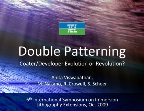
Double Patterning<br />
<strong>Coater</strong>/<strong>Developer</strong> <strong>Evolution</strong> <strong>or</strong> <strong>Revolution</strong>?<br />
Anita Viswanathan,<br />
M. Nakano, R. Crowell, S. Scheer<br />
6 th International Symposium on Immersion<br />
Lithography Extensions, Oct 2009
Outline<br />
• <strong>Evolution</strong> of CLEAN TRACK Technology<br />
• DP Implications on <strong>Coater</strong>/<strong>Developer</strong> Design<br />
• CLEAN TRACK DP Activity Update<br />
• Summary
i-line<br />
KrF / ArF<br />
Immersion<br />
<strong>Evolution</strong> of CLEAN TRACK<br />
Technology<br />
• Lens Substrate Contamination Reflectivity<br />
• Wafer Amine Edge Contamination Defectivity<br />
• Residual PEB Sensitivity Water Defects<br />
ADH Chill Coat PAB<br />
WEE EXP PEB Chill Dev<br />
ADH Chill BCT Bake Chill Coat PAB<br />
WEE Chill EXP PEB Chill Dev<br />
ADH Chill BCT Bake Chill Coat PAB Chill TCT Bake Chill WEE Rinse Chill EXP Rinse PEB Chill Dev
Double Exp<br />
Neg. Tone<br />
Develop<br />
Complexity of DP Space<br />
LELE LLE<br />
SWT<br />
Scheme 1<br />
Scheme 2<br />
Neg. Tone<br />
Develop<br />
Contact Hole<br />
Line Cutting<br />
Chemical<br />
Thermal<br />
UV Cure<br />
Vap<strong>or</strong><br />
Implant<br />
C<strong>or</strong>e Type 1<br />
C<strong>or</strong>e Type 2<br />
C<strong>or</strong>e Type 3<br />
Pitch Doubling<br />
Dual Tone<br />
Develop<br />
Neg. Tone<br />
Develop<br />
•DP techniques serve unique applications (trench, C/H, etc)<br />
• <strong>Coater</strong>/<strong>Developer</strong>s are required to supp<strong>or</strong>t multiple DP techniques<br />
simultaneously<br />
•Many approaches require dedicated coater/developer modules
1 st Exposure<br />
1 st Etch<br />
2 nd Exposure<br />
2 nd Etch<br />
1 st Exposure<br />
Freeze<br />
2 nd Exposure<br />
Etch<br />
Throughput Demand from DP<br />
ADH ADH Chill Chill BCT BCTBake Bake Chill ChillCoat CoatPABPAB Chill Chill TCT TCT Bake Bake Chill Chill WEE WEERinse Rinse Chill Chill EXP EXPRinse<br />
Rinse PEB PEB Chill Chill Dev Dev<br />
Bake<br />
BARC Gate<br />
Etch Freeze Etch<br />
Coat<br />
UV Cure<br />
Single Exposure LITHO-ETCH 19 processing steps<br />
LITHO-ETCH-LITHO-ETCH 44 processing steps<br />
LITHO-LITHO-ETCH 39 processing steps<br />
Strip<br />
Bake<br />
ADH Chill BCT Bake Chill Coat PAB Chill TCT Bake Chill WEE Rinse Chill EXP Rinse PEB Chill Dev<br />
BARC Gate<br />
Strip<br />
Etch BARC Etch Gate<br />
Strip<br />
Etch Etch<br />
Chill Coat PAB Chill TCT Bake Chill WEE Rinse Chill EXP Rinse PEB Chill Dev
The Next Generation of CLEAN TRACK<br />
f<strong>or</strong> DP:<br />
LITHIUS Pro V
Key <strong>Coater</strong>/<strong>Developer</strong> DP Concerns<br />
Process Perf<strong>or</strong>mance<br />
• Side Wall Technology<br />
• PR Slimming<br />
• LWR Reduction<br />
• Cross Line C/H<br />
• Pattern Collapse<br />
• Negative Tone Develop<br />
Cost of Ownership<br />
• Process Costs<br />
• SWT<br />
• Dual Tone DP<br />
• Tool Productivity<br />
• OEE<br />
• WPD
TEL Resist C<strong>or</strong>e SWT Overview<br />
Post<br />
Litho<br />
Clean Track<br />
ProV<br />
40nm hp<br />
CDU = 1.9nm<br />
LWR = 4.3nm<br />
BARC<br />
Trim<br />
TACTRAS<br />
VIGUS<br />
Deposit<br />
SiO 2<br />
TELINDY<br />
SiO 2<br />
Etch‐back<br />
C<strong>or</strong>e Strip<br />
TACTRAS<br />
VIGUS<br />
H/M<br />
Etch<br />
TACTRAS<br />
VIGUS<br />
20nm hp<br />
CDU = 2.0nm<br />
LWR = 2.5nm
PR Line Slimming & LWR Reduction<br />
Post<br />
Litho<br />
Clean Track<br />
Pro V<br />
PR Wet<br />
Slimming<br />
Process<br />
PR LWR<br />
Smoothing<br />
Process<br />
40nm hp<br />
CDU = 1.9nm<br />
LWR = 4.3nm<br />
New PR<br />
Process<br />
LWR data samples made by IMEC<br />
BARC<br />
Trim<br />
TACTRAS<br />
VIGUS<br />
SiO2<br />
Depo<br />
TELINDY<br />
SiO2<br />
Etch‐back<br />
C<strong>or</strong>e Strip<br />
TACTRAS<br />
VIGUS<br />
Initial Pattern Post Slimming<br />
CD=49.9nm<br />
LWR=4.9nm<br />
H=92.5nm<br />
H/M<br />
Etch<br />
TACTRAS<br />
VIGUS<br />
CD=32.8nm (-17.1nm)<br />
LWR=4.0nm (-0.9nm)<br />
H=83.3nm (-9.2nm)<br />
Initial Pattern Post Smoothing<br />
LWR3s: 3.1nm LWR3s: 2.7nm<br />
20nm hp<br />
CDU = 2.0nm<br />
LWR = 2.5nm
Freeze‐Free Posi‐Posi Process Cross Line C/H<br />
Initial Si-H-M Etch Carbon Etch TEOS Etch Ashing<br />
Samples made by TOK<br />
1 st Space<br />
2 nd Space<br />
1 st Space<br />
Average:46.18nm<br />
3σ:2.37nm<br />
2 nd Space<br />
Average:45.64nm<br />
3σ:1.91nm
TEL FIRM Impact on Pattern Collapse<br />
Coat freeze<br />
LLE L/S Patterning<br />
DIW Rinse Surfactant Rinse<br />
~170 defects<br />
due to pattern collapse<br />
~0 defects<br />
due to pattern collapse<br />
TEL FIRM has demonstrated effectiveness across multiple LLE<br />
processes.<br />
Data courtesy of IMEC<br />
Reference: Towards 26nm hp: Advances in Litho<br />
Process Litho; P. Wong
Negative Tone Development<br />
Process A —1 st Trial Defect Data<br />
Measurement Area LS RESIST BARC<br />
Classification<br />
Process A Process B Process C<br />
CDU 3σ = 1.39%<br />
DEV = 1 unit/waf<br />
CDU 3σ = 2.75%<br />
DEV = 1 unit/waf<br />
CDU 3σ = 3.2%<br />
DEV = 0.45<br />
unit/waf<br />
Defect Counts [cts/waf] 0 4 2<br />
Defect Density [cts/cm 2 ] 0.000 0.026 0.030
Key <strong>Coater</strong>/<strong>Developer</strong> DP Concerns<br />
Process Perf<strong>or</strong>mance<br />
• Spacer<br />
• PR Slimming<br />
• LWR Reduction<br />
• Cross Line C/H<br />
• Pattern Collapse<br />
• Negative Tone Develop<br />
Cost of Ownership<br />
• Process Costs<br />
• Resist C<strong>or</strong>e SWT<br />
• Dual Tone DP<br />
• Tool Productivity<br />
• Overall Equipment Efficiency<br />
(OEE)<br />
• Wafers Per Day (WPD)
Post<br />
Litho<br />
Process Costs:<br />
Non Resist C<strong>or</strong>e SWT vs. Resist C<strong>or</strong>e SWT<br />
Cost Per Patterning ($)<br />
BARC<br />
Trim<br />
SiO 2<br />
Deposition<br />
Exposure Track Etch Clean CVD<br />
Non Resist C<strong>or</strong>e SWT Resist C<strong>or</strong>e SWT<br />
SiO 2<br />
Etch‐back<br />
C<strong>or</strong>e Strip<br />
14% Savings<br />
H/M<br />
Etch<br />
CT PR Wet<br />
Slimming
Process Costs: Dual‐Tone Development<br />
Overview<br />
Reference: Expl<strong>or</strong>ation of …Dual tone<br />
Development; C. Fonseca<br />
1.26NA, Dipole<br />
(K 1 = 0.21)<br />
Current Status<br />
16nm<br />
100X diluted TMAH, PEB2: 150C/60s<br />
64nm Pitch<br />
Mask Pitch: 128nm<br />
• Demonstrated image modulation<br />
• Resolution below single exposure &<br />
develop 1.35NA scanner capability
Process Costs:<br />
Non Resist C<strong>or</strong>e SWT vs. Dual Tone<br />
Post<br />
Litho (2DEV)<br />
Cost Per Patterning ($)<br />
BARC<br />
Trim<br />
Non Resist C<strong>or</strong>e SWT Dual Tone<br />
Development<br />
H/M<br />
Etch<br />
Exposure Track Etch Clean CVD<br />
21% Savings<br />
CT PR Wet<br />
Slimming
Tool Productivity: LITHIUS Pro V<br />
OEE<br />
FOUP Exchanger<br />
System<br />
Multi cycle wafer flow<br />
control Function<br />
PRIME Cascade<br />
Transfer Control<br />
Additional OEE<br />
improvement items<br />
DP Process Capability<br />
Throughput / Footprint<br />
High T.P 250wph<br />
capability and<br />
Flexible Configuration<br />
LITHIUS Pro vs LITHIUS Pro V<br />
25% Greater Throughput with only<br />
10% Footprint Increase<br />
New Process<br />
Wet Slimming<br />
Capability<br />
(PR Pattern Trimming)<br />
Freezing Process<br />
Capability f<strong>or</strong> LLE<br />
Negative Tone<br />
Development Process<br />
Capability<br />
FIRM Process f<strong>or</strong><br />
Defect reduction<br />
Smoothing Process f<strong>or</strong><br />
LWR Improvement<br />
(Future Upgrade)<br />
Pro V<br />
PIR<br />
SRS<br />
SRS
Tool Productivity: Overall Equipment<br />
Efficiency (OEE) Improvement<br />
Conventional LITHIUS Pro<br />
(current)<br />
10% Increase<br />
LITHIUS Pro V
Tool Productivity: Wafers Per Day<br />
(WPD) Improvement<br />
OEE Improvement<br />
Throughput Increase<br />
LITHIUS Pro<br />
180 wph<br />
32%<br />
LITHIUS Pro V<br />
220 wph<br />
54%<br />
LITHIUS Pro V<br />
250 wph
Summary<br />
• DP processes are chosen by technology<br />
perf<strong>or</strong>mance, customer device / layer type, and<br />
integration strategy, creating a complex space<br />
• TEL’s objective is to be a partner, regardless of<br />
the DP technology used, in helping our customers<br />
to:<br />
– Establish w<strong>or</strong>ld class process perf<strong>or</strong>mance<br />
– Achieve the highest productivity with lowest process<br />
cost
• TEL:<br />
Acknowledgements<br />
– S. Shimura, T. Kawasaki, S. Nat<strong>or</strong>i, A. Hara, K. Hontake, T.<br />
Niwa, C. Fonseca, K. Nafus, H. Yaegashi<br />
• IMEC<br />
– P. Wong, R. Gronheid