DS 7-7R 17-12R Semiconductor Fabrication Facilities ... - FM Global
DS 7-7R 17-12R Semiconductor Fabrication Facilities ... - FM Global
DS 7-7R 17-12R Semiconductor Fabrication Facilities ... - FM Global

Create successful ePaper yourself
Turn your PDF publications into a flip-book with our unique Google optimized e-Paper software.
7-<strong>7R</strong><br />
REFERENCE DOCUMENT<br />
<strong>17</strong>-<strong>12R</strong> SEMICONDUCTOR FABRICATION FACILITIES<br />
Page 18<br />
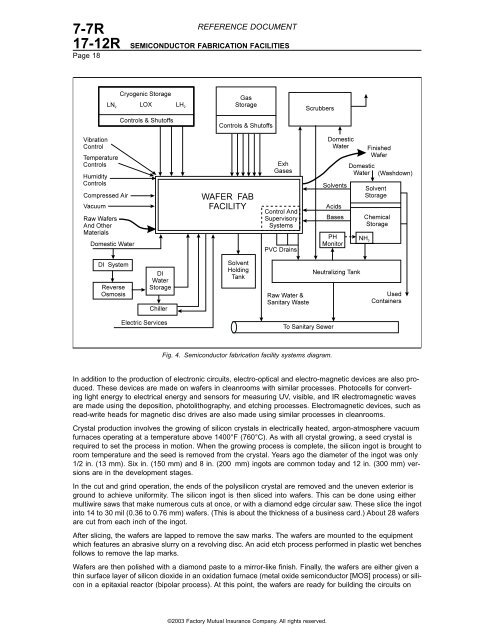
Fig. 4. <strong>Semiconductor</strong> fabrication facility systems diagram.<br />
In addition to the production of electronic circuits, electro-optical and electro-magnetic devices are also produced.<br />
These devices are made on wafers in cleanrooms with similar processes. Photocells for converting<br />
light energy to electrical energy and sensors for measuring UV, visible, and IR electromagnetic waves<br />
are made using the deposition, photolithography, and etching processes. Electromagnetic devices, such as<br />
read-write heads for magnetic disc drives are also made using similar processes in cleanrooms.<br />
Crystal production involves the growing of silicon crystals in electrically heated, argon-atmosphere vacuum<br />
furnaces operating at a temperature above 1400°F (760°C). As with all crystal growing, a seed crystal is<br />
required to set the process in motion. When the growing process is complete, the silicon ingot is brought to<br />
room temperature and the seed is removed from the crystal. Years ago the diameter of the ingot was only<br />
1/2 in. (13 mm). Six in. (150 mm) and 8 in. (200 mm) ingots are common today and 12 in. (300 mm) versions<br />
are in the development stages.<br />
In the cut and grind operation, the ends of the polysilicon crystal are removed and the uneven exterior is<br />
ground to achieve uniformity. The silicon ingot is then sliced into wafers. This can be done using either<br />
multiwire saws that make numerous cuts at once, or with a diamond edge circular saw. These slice the ingot<br />
into 14 to 30 mil (0.36 to 0.76 mm) wafers. (This is about the thickness of a business card.) About 28 wafers<br />
are cut from each inch of the ingot.<br />
After slicing, the wafers are lapped to remove the saw marks. The wafers are mounted to the equipment<br />
which features an abrasive slurry on a revolving disc. An acid etch process performed in plastic wet benches<br />
follows to remove the lap marks.<br />
Wafers are then polished with a diamond paste to a mirror-like finish. Finally, the wafers are either given a<br />
thin surface layer of silicon dioxide in an oxidation furnace (metal oxide semiconductor [MOS] process) or silicon<br />
in a epitaxial reactor (bipolar process). At this point, the wafers are ready for building the circuits on<br />
©2003 Factory Mutual Insurance Company. All rights reserved.