Photovoltaics - IPHT Jena
Photovoltaics - IPHT Jena
Photovoltaics - IPHT Jena

You also want an ePaper? Increase the reach of your titles
YUMPU automatically turns print PDFs into web optimized ePapers that Google loves.
Institute of Photonic Technology<br />
Albert-Einstein-Straße 9<br />
07745 <strong>Jena</strong><br />
PD Dr. rer. nat. habil. F. Falk<br />
Tel. 03641 206438<br />
e-mail: fritz.falk@ipht-jena.de<br />
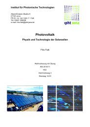
<strong>Photovoltaics</strong><br />
Physics and Technology of Solar Cells<br />
Figures and Tables<br />
Fritz Falk<br />
Institute of Photonic Technology<br />
Elective Course Master Photonics<br />
WS 2010/11<br />
HS3, Helmholtzweg 3<br />
Tuesday 14:00 - 16:00
Contents<br />
Manuscript in German: www. ipht-jena.de 6Institut 6 Lehre<br />
1 Energy Consumption and its Consequences<br />
1.1 Energy Consumption Yesterday, Today and Tomorrow<br />
1.2 Supply of Energy Sources<br />
1.3 The Green House Effect<br />
1.4 Energy Scenarios<br />
1.5 Requirements on Solar Cells for Different Applications<br />
2 Insolation<br />
3 Basics of <strong>Photovoltaics</strong><br />
3.1 History of <strong>Photovoltaics</strong><br />
3.2 Basic Principles of Solar Cells<br />
3.3 The Influence of the Band Gap<br />
3.4 Absorption Coefficient<br />
3.5 I-V-Diagram of a Solar Cell<br />
3.6 Overview on Solar Cell Types<br />
4 Semiconductors I: Equilibrium<br />
4.1 Crystal Structure<br />
4.2 Band Diagram<br />
4.3 Dynamics of Electrons<br />
4.4 Electrons and Holes<br />
4.5 Fermi Distribution and Carrier Densities in Undoped Semiconductors<br />
4.6 Doped Semiconductors<br />
4.7 Conductivity and Hall Effect<br />
4.8 Space Charges, Fields, Currents<br />
4.9 Inhomogeneities in Equilibrium<br />
5 Semiconductors II: Non-Equilibrium<br />
5.1 Optical Absorption<br />
5.2 Carriers in Non-Equilibrium: Quasi-Fermi Levels<br />
5.3 Generation and Recombination<br />
5.4 Balance of Charges in Non-Equilibrium<br />
5.5 p-n-Junction with External Voltage<br />
5.6 p-n-Junction under Illumination: Solar Cell<br />
5.7 Thermodynamics of Solar Cells and Efficiency Thresholds<br />
6 Solar Cell Types I: Wafer Cells<br />
6.1 Single Crystalline Silicon Solar Cells<br />
6.2 Multicrystalline Silicon Solar Cells<br />
7 Solar Cell Types II: Thin-Film Cells<br />
7.1 General Scheme of Thin-Film Cells<br />
7.2 Amorphous Silicon Thin-Film Cells<br />
7.3 Crystalline Silicon Thin-Film Cells<br />
7.4 Gallium Arsenide Cells<br />
7.5 CdTe Cells<br />
7.6 CIGS Cells<br />
7.7 Polymer Cells<br />
7.8 Grätzel Cell<br />
Contents F. Falk, <strong>Photovoltaics</strong> WS 2010/11
- 3 -<br />
1 Energy Consumption and ist Consequences<br />
Fig. 1.1: Worldwide energy consuption<br />
Table 1.1: Share of primary energy sources used for generation of electricity 2008)<br />
pit coal brown coal oil gas nuclear water<br />
Germany 21% 24% 1% 13% 24% 4%<br />
world 41% 6% 21% 14% 16%<br />
Fig. 1.2: Predicted energy consumption worldwide by energy sources( Shell Study 1999)<br />
1 Energy Consumption and ist Consequences F. Falk, <strong>Photovoltaics</strong> WS 2010/11
- 4 -<br />
Table 1.2: Reserves (today economically useful) and resources (today not economivally useful)<br />
of energy sources, and time until they are expected to be used up (as of 2004, data from: J.P.<br />
Gerling, F.-W. Wellmer, Chemie in unserer Zeit 39 (2005), 236)<br />
energy source today’s<br />
share<br />
reserves<br />
10 21 J<br />
ressources<br />
10 21 J<br />
reserves to<br />
last (years)<br />
coal 0,232 20 117 65 125<br />
oil 0,342 9 14 34 58<br />
natural gas 0,196 6 7 38 57<br />
gas and<br />
methane hydrate<br />
0,196 6 55 38 104<br />
nuclear* 0,062 1 10 25 86<br />
nuclear fusion 0<br />
* without breeder technology<br />
Fig. 1.3: Change of CO 2 concentration in the atmosphere<br />
(from Physics today, Aug. 2002)<br />
ressources to<br />
last (years)<br />
1 Energy Consumption and ist Consequences F. Falk, <strong>Photovoltaics</strong> WS 2010/11
- 5 -<br />
Fig. 1.4: Increase of mean temperature of the atmosphere near ground<br />
(IPCC-Report 2007)<br />
Fig. 1.5: Predicted temperature change of the earth’s atmosphere according to different<br />
models and different assumptions compared to observations (from: IPCC Report 2001)<br />
1 Energy Consumption and ist Consequences F. Falk, <strong>Photovoltaics</strong> WS 2010/11
- 6 -<br />
Fig. 1.6: Scenarios for the expected temparture change (from IPCC Report 2007)<br />
Table 1.3: Share of renewable energy sources for generation of electricity in Germany 2009<br />
total 16%<br />
water 3,3%<br />
wind 6,4%<br />
photovoltaics 1,0%<br />
geothermal 0,02%<br />
biomass 4,4%<br />
waste 0,9%<br />
1 Energy Consumption and ist Consequences F. Falk, <strong>Photovoltaics</strong> WS 2010/11
- 7 -<br />
Table 1.4: Production and market share of solar cells by countries<br />
country produktion<br />
share<br />
2009<br />
market<br />
share<br />
2008<br />
China 38% 0,2%<br />
share in totally<br />
installed<br />
capacitiy 2008<br />
Germany 15% 27% 40%<br />
Japan 12,5% 4% 16%<br />
Taiwan 12,2<br />
USA 4,4% 6% 9%<br />
Spain 3% 48% 25%<br />
Tab. 1.5: Produktion share of solar cells by companies (2009, Photon International 3/2010)<br />
Produktionsanteil Firmen<br />
First Solar (USA, D) 8,9%<br />
Suntech Power (China) 5,7%<br />
Q-Cells (D, Thalheim S-A) 4,8%<br />
Sharp (JP) 4,8%<br />
Yingli (China) 4,3%<br />
JA Solar (China) 4,2%<br />
Trina (China) 3,2%<br />
Sunpower (Philippinen) 3,2%<br />
Gintech (Taiwan) 3,0%<br />
Kyocera (JP) 3,2%<br />
1 Energy Consumption and ist Consequences F. Falk, <strong>Photovoltaics</strong> WS 2010/11
2 Insolation<br />
Fig. 2.1: Radiation density<br />
above atmosphere [Würfel]<br />
Upper part:<br />
referred to energy interval<br />
Lower part:<br />
Referred to wavelength interval<br />
Fig. 2.2: Radiation density on<br />
ground [Hu]<br />
-8 -<br />
2 Sonneneinstrahlung F. Falk, Photovoltaik WS 2010/11
-9 -<br />
Fig. 2.3: Insolation as depending on time of the year and on inclination of solar the<br />
cell [Hu]<br />
Fig. 2.4: [Hu]<br />
2 Sonneneinstrahlung F. Falk, Photovoltaik WS 2010/11
- 10 -<br />
2 Sonneneinstrahlung F. Falk, Photovoltaik WS 2010/11<br />
Fig. 2.5: Average yearly global irradiation
- 11 -<br />
Fig. 2.6: Average yearly global irradiation in Germany<br />
2 Insolation F. Falk, <strong>Photovoltaics</strong> WS 2010/11
3 Basics of <strong>Photovoltaics</strong><br />
- 12 -<br />
1 Absorption of light: cell is not transparent<br />
Example<br />
Si wafer cell<br />
2 Generation of charge carriers<br />
electrons & holes<br />
3 Carriers are mobile: diffusion<br />
6<br />
4<br />
5<br />
Carrier life-time high enough<br />
Charge separation<br />
p-n junction<br />
hetero junction<br />
p-Si<br />
3<br />
4<br />
1,2<br />
+<br />
3<br />
4<br />
6 Carrier leave cell<br />
Space charge region 5<br />
contacts<br />
n-Si<br />
Fig. 3.1: Basic processes in a solar cell<br />
conduction band<br />
band gap<br />
E g<br />
valence band<br />
? ? ? ? ? ?<br />
hνE g<br />
3 Basics of <strong>Photovoltaics</strong> F. Falk, <strong>Photovoltaics</strong> WS 2010/11<br />
? ? ? ? ? ?<br />
fs<br />
fs<br />
loss<br />
µs<br />
loss<br />
Fig. 3.2: Photon absorption an carrier excitation in a semiconductor<br />
6<br />
electrons<br />
holes<br />
- contact<br />
+ contact
Table 3.1: Band gaps of semiconductors<br />
- 13 -<br />
Fig. 3.3: Limits for solar cell efficiency as depending on the band gap. Upper left: Ultimate<br />
efficiency,upper right: Shockley-Queisser-limit, below: semiempirical efficiency<br />
[Hu]<br />
Semiconductor Si a-Si GaAs CdTe CuInSe2 Eg/eV 1,12 1,6...1,7 1,43 1,43 1,05<br />
3 Basics of <strong>Photovoltaics</strong> F. Falk, <strong>Photovoltaics</strong> WS 2010/11
- 14 -<br />
Fig. 3.4: Efficiency of a two junction tandem solar cell as depending on<br />
both the band gaps [Lewerenz]<br />
Fig. 3.5: Theoretical efficiency of a tandem solar cell with n<br />
junctions and optimized band gaps under AM0 irradiatopn<br />
[Lewerenz]<br />
3 Basics of <strong>Photovoltaics</strong> F. Falk, <strong>Photovoltaics</strong> WS 2010/11
- 15 -<br />
Fig. 3.6: Absorptions coefficient semiconductors [Hu]<br />
3 Basics of <strong>Photovoltaics</strong> F. Falk, <strong>Photovoltaics</strong> WS 2010/11
- 16 -<br />
Table 3.2: Types of solar cells: maximum efficiency under AM1.5 [(M.A.<br />
Green et al., Solar Cell Efficiency Tables (Version 36), Prog. Photovolt. 18 (2010), 346] and<br />
production share in 2009 [Photon Int. 2/2009]<br />
Type Efficiency<br />
Lab/Module<br />
%<br />
Wafer Cells<br />
Production<br />
share<br />
2009<br />
%<br />
Further Work<br />
single crystalline Si 25.0/13-17 341 Processes,<br />
Cell Configurations<br />
multi-crystalline Si 20,4/11-15 483 Processes,<br />
Cell Configurations<br />
Thin Film Cells<br />
amorphous Si 10.1/5-8 61 Low cost processes<br />
CdTe 16.7/9-11 90 Higher efficiency in<br />
production<br />
CIS/CIGS 19.4/10-11 17 Higher efficiency in<br />
production<br />
nanocrystalline Si 10,1/... - Research<br />
micro-/polycrystalline Si 10,5/7 - Research<br />
Grätzel 10,4/... - Research, processes<br />
Polymers 5,1/... - Research, more stable<br />
3 Basics of <strong>Photovoltaics</strong> F. Falk, <strong>Photovoltaics</strong> WS 2010/11
- 17 -<br />
4 Semiconductors I: Equilibrium<br />
Diamond lattice:<br />
fcc with base<br />
Zink-blende lattice (cubic) Wurtzite lattice (hexagonal)<br />
Zink-blende lattice Wurtzite lattice<br />
Fig. 4.1: Semiconductor lattices<br />
4 Semiconductors I: Equilibrium F. Falk, <strong>Photovoltaics</strong> WS 2010/11
- 18 -<br />
Fig. 4.2: First Brillouin zone of diamond lattice<br />
Table. 4.1: Band gaps of semiconductors (at room temperature)<br />
Si a-Si GaAs CdTe CuInSe2<br />
E g/eV<br />
1,12 1,6...1,7 1,43 1,43 1,05<br />
Fig. 4.3: Band structure of Si [Enderlein]<br />
4 Semiconductors I: Equilibrium F. Falk, <strong>Photovoltaics</strong> WS 2010/11
Fig. 4.4: Band structure of GaAs<br />
Fig. 4.5: Band structure of CdTe<br />
- 19 -<br />
4 Semiconductors I: Equilibrium F. Falk, <strong>Photovoltaics</strong> WS 2010/11
- 20 -<br />
Fig. 4.6: Basic structure of an electron band (left) and electron motion under a constant force<br />
(right)<br />
Fig. 4.8: Electrical conductivity of metals<br />
Fig. 4.7: Density of states in crystalline silicon (left) and in amorphous silicon (right)<br />
4 Semiconductors I: Equilibrium F. Falk, <strong>Photovoltaics</strong> WS 2010/11
Fig. 4.9: Fermi distribution for<br />
different temperatures<br />
- 21 -<br />
Fig. 4.10: Density of states (left), Fermi distribution (middle) and density of occupied states<br />
(right)<br />
4 Semiconductors I: Equilibrium F. Falk, <strong>Photovoltaics</strong> WS 2010/11
- 22 -<br />
Table 4.2: Band gap,, effective mass and carrier density in intrinsic semiconductors<br />
semiconductor Si GaAs<br />
E g/eV<br />
1,12 1,43<br />
m /m 1,08 0,067<br />
nZ 0<br />
m /m 0,55 0,47<br />
pZ 0<br />
-3 n i/cm<br />
at 300 K<br />
10 6<br />
10 10<br />
Table 4.3: Energy level of donors and acceptors in silicon<br />
donors E-E c D/meV acceptors EA-E v/meV<br />
P 45 B 44<br />
As 53 Al 68<br />
Sb 42 Ga 72<br />
Bi 71 In 155<br />
Fig. 4.11: Fermi level as depending on temperature for different<br />
doping levels (n doping increasing from 1 to 3)<br />
4 Semiconductors I: Equilibrium F. Falk, <strong>Photovoltaics</strong> WS 2010/11
- 23 -<br />
Fig. 4.12: Carrier density in n- doped semiconductors as a function of inverse temperature<br />
Fig. 4.13: Carrier density as a function of inverse temperature in n-doped semiconductors<br />
which contain also p-dopands<br />
4 Semiconductors I: Equilibrium F. Falk, <strong>Photovoltaics</strong> WS 2010/11
- 24 -<br />
15 -3<br />
Table 4.4: Carrier mobilities at 300 K (for Si and GaAs dopand density 10 cm )<br />
Si GaAs CdTe CuInSe2 a-Si<br />
2 -1 -1 ì /cm V s 1350 8800 600 320 0,1...1<br />
n<br />
2 -1 -1 -3<br />
ì /cm V s 500 400 10 10 ...0,03<br />
p<br />
Fig. 4.14: Mobility of electrons and holes at 300 K as<br />
depending on doping level[Enderlein]<br />
Fig. 4.15: Mobilities for different doping levels of silicon as depending on temperature<br />
[Enderlein]<br />
4 Semiconductors I: Equilibrium F. Falk, <strong>Photovoltaics</strong> WS 2010/11
- 25 -<br />
Fig. 4.17: Resistivity of n- or p-doped silicon at 300 K<br />
[Colinge]<br />
Fig. 4.18: Measurement arrangement for Hall effect<br />
Fig. 4.16: Conductivity of pure intrinsic Si and Ge<br />
as depending on temperature [Enderlein]<br />
4 Semiconductors I: Equilibrium F. Falk, <strong>Photovoltaics</strong> WS 2010/11
- 26 -<br />
Table 4.5: Debye length in instrinsic semiconductors at 300 K<br />
semiconductor Si GaAs<br />
-3<br />
l D/cm<br />
1,15�10 0,116<br />
Fig. 4.19: Band bending near the surface of an intrinsic semiconductor due to surface charges<br />
4 Semiconductors I: Equilibrium F. Falk, <strong>Photovoltaics</strong> WS 2010/11
- 27 -<br />
Fig. 4.20: Band bending near the surface of an<br />
n-doped semiconductor due to surface charges<br />
4 Semiconductors I: Equilibrium F. Falk, <strong>Photovoltaics</strong> WS 2010/11
Fig. 4.21: Band diagram of a p-n-junction<br />
- 28 -<br />
Table 4.6: Diffusion potential at a p-n-Übergang in silicon at 300 K in case N A=ND -3<br />
N A=N D/cm<br />
15<br />
10<br />
16<br />
10<br />
17<br />
10<br />
18<br />
10<br />
19<br />
10<br />
20<br />
10<br />
V /V 0,542 0,654 0,766 0,878 0,991 1,103<br />
D<br />
w 1,4 µm 440 nm 140 nm 44 nm 14 nm 4,4 nm<br />
Fig. 4.22: Band diagram, carrier densities, and space charge density at a p-n-junction<br />
4 Semiconductors I: Equilibrium F. Falk, <strong>Photovoltaics</strong> WS 2010/11
- 29 -<br />
4 Semiconductors I: Equilibrium F. Falk, <strong>Photovoltaics</strong> WS 2010/11<br />
E 0 or EFig. 0-e�:<br />
4.23: vacuum Metal/se<br />
leve
- 30 -<br />
Fig. 4.24: Band diagram of a semiconductor heterojunction<br />
without interface charges. Above: before contact, below:<br />
after contact<br />
4 Semiconductors I: Equilibrium F. Falk, <strong>Photovoltaics</strong> WS 2010/11
- 31 -<br />
5 Semiconductors II: Non-Equilibrium<br />
Fig. 5.2: Quasi Fermi levels under illumination<br />
Fig. 5.1: Tauc-Plot of amorphous silicon,<br />
deposited at different temperatures<br />
[Diss. C. Horbach, KFA Jülich]<br />
5 Halbleiter II: Nichtgleichgewicht F. Falk, Photovoltaik WS 2010/11
- 32 -<br />
Fig. 5.3: Carrier life time in silicon as depending on<br />
excess carrier density [Lewerenz u. Jungblut]<br />
5 Halbleiter II: Nichtgleichgewicht F. Falk, Photovoltaik WS 2010/11
Reverse bias<br />
n-type +<br />
Forward bias<br />
n-type -<br />
without external voltage<br />
In equilibrium<br />
- 33 -<br />
5 Halbleiter II: Nichtgleichgewicht F. Falk, Photovoltaik WS 2010/11<br />
Fig. 5.4: p-n-junction under external bias
- 34 -<br />
Fig. 5.5: I-V-Curves of diodes (be aware of different<br />
voltage scales in case of reverse and forward bias)<br />
Fig. 5.6: I-V-curves of diodes, logarithmic scale for current<br />
5 Halbleiter II: Nichtgleichgewicht F. Falk, Photovoltaik WS 2010/11
- 35 -<br />
Fig. 5.7: Width of space charge region of a silicon p-njunction<br />
as depending on bias<br />
N A=N D=10 16 cm -3 , g=12<br />
metal contact<br />
absorber<br />
Fig. 5.8: Scheme of a silicon wafer cell<br />
anti-reflection coating<br />
back contact (Al)<br />
emitter<br />
5 Halbleiter II: Nichtgleichgewicht F. Falk, Photovoltaik WS 2010/11
in the dark<br />
illuminated but without<br />
equilibrium between<br />
p- and n-side<br />
- 36 -<br />
illuminated, when equilibrium<br />
between p- and n-side is reached<br />
Fig. 5.9: Band diagram of a silicon wafer cell<br />
5 Halbleiter II: Nichtgleichgewicht F. Falk, Photovoltaik WS 2010/11
Fig. 5.10: I-V-curve of a solar cell in the dark<br />
and under illumination<br />
- 37 -<br />
5 Halbleiter II: Nichtgleichgewicht F. Falk, Photovoltaik WS 2010/11
- 38 -<br />
Fig. 5.11: Fill factor and efficiency of a silicon wafer cell as depending on the ratio i p/i s if<br />
illuminated by a wavelength of 500 nm at 300 K<br />
5 Halbleiter II: Nichtgleichgewicht F. Falk, Photovoltaik WS 2010/11
Fig. 5.12: Circuit diagram of a solar cell<br />
Fig. 5.13: Influence of series resistance on the<br />
I-V-curve of a solar cell<br />
- 39 -<br />
Fig. 5.14: Influence of a shunt (parallel resistance)<br />
on the I-V-curve of a solar cell<br />
5 Halbleiter II: Nichtgleichgewicht F. Falk, Photovoltaik WS 2010/11
- 40 -<br />
6 Types of Solar Cells I: Wafer Cells<br />
Fig. 6.1: Scheme of a single crystalline silicon wafer cell<br />
Fig. 6.2: Czochralski method to grow silicon single crystals<br />
6 Solarzellentypen I: Waferzellen F. Falk, Photovoltaik WS 2010/11
Fig. 6.3: Wire saw for wafering<br />
- 41 -<br />
Fig. 6.4: Phosphorus doping profile generated by annealing at<br />
950�C for different times [Goetzberger]<br />
6 Solarzellentypen I: Waferzellen F. Falk, Photovoltaik WS 2010/11
- 42 -<br />
Fig. 6.5: ReCombination activity of various species in p- und<br />
n-doped silicon,Shown is the product of resulting carrier life<br />
time and foreign atom concentration<br />
6 Solarzellentypen I: Waferzellen F. Falk, Photovoltaik WS 2010/11
- 43 -<br />
Fig. 6.6: Open circuit voltage as depending on diffusion<br />
length for different values of surface recombination<br />
velocity [Goetzberger]<br />
Fig. 6.7: Short circuit current as depending on<br />
diffusion length for different values of surface<br />
recombination velocity [Goetzberger]<br />
6 Solarzellentypen I: Waferzellen F. Falk, Photovoltaik WS 2010/11
- 44 -<br />
Fig. 6.8: Solar cell efficiency as depending on absorber doping level for<br />
different wafer thickness [Goetzberger]<br />
Fig. 6.9: Band diagram of a cell with back surface field<br />
6 Solarzellentypen I: Waferzellen F. Falk, Photovoltaik WS 2010/11
- 45 -<br />
Fig. 6.10: Open circuit volatge as depending on the depth and<br />
maximum concentration of back surface field doping [Goetzberger]<br />
Fig. 6.11: Reflection at a silicon surface covered with no, 1, and 2<br />
antireflection coatings as depending on light wavelength<br />
[Goetzberger]<br />
6 Solarzellentypen I: Waferzellen F. Falk, Photovoltaik WS 2010/11
- 46 -<br />
Fig. 6.12: Internal quantum efficiency as depending on<br />
dislocation density for two different values of<br />
recombination strength [Möller]<br />
Fig. 6.13: EFG method for growing silicon sheets<br />
Fig. 6.14: RGS method to produce silicon foils<br />
6 Solarzellentypen I: Waferzellen F. Falk, Photovoltaik WS 2010/11
- 48 -<br />
7 Types of Solar Cells II: Thin Film Cells<br />
Fig. 7.1: Integrated series connection in amorphosu silicon thin film solar cells<br />
Fig. 7.2: pin-type amorphous silicon solar cell<br />
7 Types of Solar Cells II: Thin Film Cells F. Falk, <strong>Photovoltaics</strong> WS 2010/11
without contact<br />
with contact<br />
- 49 -<br />
Fig. 7.3: band diagram of a pin-type solar cell. Above:<br />
before conatct of differently doped regions, below: after<br />
contact<br />
p-type<br />
n-type<br />
nominally<br />
undoped<br />
Fig. 7.4: Influence of doping gas concemtration<br />
during CVD of amorphous silicon on conductivity<br />
7 Types of Solar Cells II: Thin Film Cells F. Falk, <strong>Photovoltaics</strong> WS 2010/11
- 50 -<br />
Fig. 7.5: Open circuit voltage of crystalline silicon thin film solar<br />
cells as depending on grain size<br />
[L. Carnel et al., 4th WCPEC 2006,1449]<br />
Fig. 7.6: Efficiency of crystalline silicon thin film solar cells as depending on grain size [J.<br />
Werner, Tech. Digest 13 th Sunshine Workshop Thin Film Solar Cells,Tokyo 2000, 41]<br />
7 Types of Solar Cells II: Thin Film Cells F. Falk, <strong>Photovoltaics</strong> WS 2010/11
- 51 -<br />
Fig. 7.7: Light trapping structures in thin film solar cells<br />
Fig. 7.8: Cell concept of a multicrystalline silicon thin film<br />
solar cell developed at <strong>IPHT</strong><br />
7 Types of Solar Cells II: Thin Film Cells F. Falk, <strong>Photovoltaics</strong> WS 2010/11
- 52 -<br />
7 Types of Solar Cells II: Thin Film Cells F. Falk, <strong>Photovoltaics</strong> WS 2010/11
- 53 -<br />
Fig. 7.10: Transmission electron microskopic image of a<br />
nanocrystalline silicion layer prepared from amorphous<br />
silicon by excimer laser irradiation (248 nm wavelength , 25<br />
ns pulse duration)<br />
Fig. 7.11: Seed layer consisiting of larges silicon crystals<br />
prepared by melting amorphous silicon by a cw-laser;<br />
melting time 1 ms (optical micrograph)<br />
7 Types of Solar Cells II: Thin Film Cells F. Falk, <strong>Photovoltaics</strong> WS 2010/11
- 54 -<br />
Fig. 7.12: LLC process: Layered Laser Crystallization<br />
absorber<br />
seed<br />
Fig. 7.13: TEM cross section of a LLClayer<br />
demonstrating epitaxy<br />
7 Types of Solar Cells II: Thin Film Cells F. Falk, <strong>Photovoltaics</strong> WS 2010/11
concentration/cm -3<br />
1E20<br />
1E19<br />
1E18<br />
1E17<br />
emitter<br />
- 55 -<br />
Concentration profiles by SIMS<br />
P<br />
absorber seed glass<br />
1E16<br />
0,0 0,5 1,0 1,5 2,0<br />
depth/µm<br />
Fig. 7.14: Doping profiles of B and B in ann LLC cell measured by SIMS<br />
Fig. 7.15: GaAs solar cell<br />
7 Types of Solar Cells II: Thin Film Cells F. Falk, <strong>Photovoltaics</strong> WS 2010/11<br />
B
Table 7.1: Properties of CdTe and CdS<br />
n-CdS p-CdTe<br />
E g/eV 2,4 1,5<br />
P/eV 4,5 4,3<br />
- 56 -<br />
Dotierung N D=2@10 17 cm -3 N A=8@10 15 cm -3<br />
Fig. 7.17: CdTe solar cell<br />
sun light<br />
Fig. 7.16: Band diagram of a CdTe solar cell [Lewerenz]<br />
back contact<br />
CdTe layer (5 µm)<br />
CdS layer (100 nm)<br />
TCO layer (250 nm)<br />
glass substrate<br />
7 Types of Solar Cells II: Thin Film Cells F. Falk, <strong>Photovoltaics</strong> WS 2010/11
- 57 -<br />
Fig. 7.18: Phase diagram of CdTe [Landolt-Börnstein N.S.<br />
III/17d]<br />
Fig. 7.19: I-V-curve (above) and quantum<br />
efficiency (below) of a CdTe solar cell [D.<br />
Bonnet in Schmid]<br />
7 Types of Solar Cells II: Thin Film Cells F. Falk, <strong>Photovoltaics</strong> WS 2010/11
Fig. 7.20: Phasen diagram of CdTe/CdCl 2<br />
[M. Burgelmann, Appl. Phys. A 69 (1999),<br />
1499]<br />
- 58 -<br />
Fig. 7.21: I-V-curves of CdTe solar cells with and without<br />
CdCl 2 treatment<br />
[R.W. Birkmire, E. Eser, Ann. Rev. Mater. Sci. 27 (1997), 625]<br />
7 Types of Solar Cells II: Thin Film Cells F. Falk, <strong>Photovoltaics</strong> WS 2010/11
Fig. 7.23: CIGS solar cell<br />
Table 7.2: Data of CuInSe 2 und CdS<br />
n-CdS p-CuInSe2 Eg/eV 2,4 1,05<br />
P/eV 4,5 4,6<br />
Dotierung N D=2@10 17 cm -3<br />
- 59 -<br />
N A=10 16 cm -3<br />
Fig. 7.22: Lattice parameters and band gaps in the CIGS system<br />
[H.W. Schock in Schmid; und wie Abb. 7.21]<br />
7 Types of Solar Cells II: Thin Film Cells F. Falk, <strong>Photovoltaics</strong> WS 2010/11
- 60 -<br />
Fig. 7.24: Band diagram of a CIGS solar cell; above: before<br />
contact, below:after contact [Lewerenz]<br />
Fig. 7.25: Structure of PPV<br />
poly phenylene vinylene<br />
7 Types of Solar Cells II: Thin Film Cells F. Falk, <strong>Photovoltaics</strong> WS 2010/11
- 61 -<br />
Fig. 7.26: Polymer solar cell using TiO x<br />
[A.C. Arango et al., Adv. Mater. 12 (2000), 1689]<br />
Fig. 7.27: Absorption and quantum efficiency of a<br />
polymer cell according to Fig.7.26<br />
7 Types of Solar Cells II: Thin Film Cells F. Falk, <strong>Photovoltaics</strong> WS 2010/11
enlargement<br />
X 1<br />
X 10 3<br />
X 10 6<br />
X 10 8<br />
- 62 -<br />
Fig. 7.28: Grätzel solar cell in different enlargements<br />
glass<br />
transparent contact<br />
electrolyte<br />
TiO 2 nanocrystals<br />
transparent conatct<br />
glass<br />
dye<br />
electrolyte<br />
TiO 2 nanocrystals<br />
(20 nm)<br />
carbon<br />
nitrogen<br />
Oxygen<br />
sulfur<br />
hydrogen<br />
ruthenium<br />
7 Types of Solar Cells II: Thin Film Cells F. Falk, <strong>Photovoltaics</strong> WS 2010/11
- 63 -<br />
Fig. 7.29: I-V-curve of a Grätzel dye solar cell<br />
[M. Grätzel, A.J. McEnvoy, 14th Europ. PSEC<br />
1997, 1820]<br />
7 Types of Solar Cells II: Thin Film Cells F. Falk, <strong>Photovoltaics</strong> WS 2010/11
References<br />
A. Goetzberger, V.U. Hoffmann, Photovoltaic Solar Energy Generation, Berlin: Springer<br />
2005<br />
Overview on technology and systems, not so much physics<br />
Solar Cells: Materials, Manufacture and Operation, T. Markvart, L. Castañer eds., Oxford:<br />
Elsevier 2005<br />
Practical Handbook of <strong>Photovoltaics</strong>: Fundamentals and Applications, T. Markvart,<br />
L. Castañer eds., Oxford: Elsevier 2003<br />
P. Würfel, Physics of solar cells, Weinheim: Wiley-VCH, 2nd ed. 2009<br />
Short introduction with emphasis on thermodynamics<br />
H.J. Möller, New Materials: Semiconductors for Solar Cells, in: Handbook of Semiconductor<br />
Technology, Vol. I, K.A. Jackson, W. Schröter eds., Weinheim: Wiley-VCH 2000, S.<br />
715-769<br />
Clean Electricity from <strong>Photovoltaics</strong>, M.D. Archer, R. Hill eds., London: Imperial College<br />
Press 2001<br />
Handbook of Photovoltaic Science and Engineering, A. Luque, S. Hegedus eds., Chichester:<br />
Wiley 2003<br />
Mostly technology<br />
C. Hu, R.M. White, Solar Cells, New York: McGraw-Hill 1983<br />
R. Brendel, Thin-Film Crystalline Silicon Solar Cells, Weinheim: Wiley-VCH 2005<br />
J.P. Collinge, C.A. Collinge, Physics of Semiconductor Devices, Boston: Kluwer Acad. Publ.<br />
2002<br />
Thin-Film Solar Cells, Y. Hamakawa ed., Berlin: Springer 2004<br />
A. Goetzberger, C. Hebling, H.-W. Schock: Photovoltaic Materials, History, Status and<br />
Outlook, Mater. Sci. Eng. R 40 (2003), 1-46<br />
M.A. Green, Third Generation <strong>Photovoltaics</strong>, Berlin: Springer 2006<br />
Visions for high efficiency solar cells making use of new concepts<br />
K. Seeger, Semiconductor Physics: An Introduction, Berlin: Springer 9 2004<br />
References F. Falk, <strong>Photovoltaics</strong> WS 2010/11
R. Enderlein, N.J.M. Horing: Fundamentals of Semiconductor Physics and Devices<br />
Singapore: World Scientific 1999<br />
H.J. Möller, Semiconductors for Solar Cells, Boston: Artech House 1992<br />
A lot of information on defects (properties and consequences)<br />
Material Parameters<br />
Landolt-Börnstein, Numerical data and functional relationships in science and technology,<br />
New Series, Springer, Berlin, Group III, Vols.17a-i, 22a,b<br />
Properties of Silicon, EMIS Datarevies Series No. 4, INSPEC 1988<br />
Properties of Amorphous Silicon, EMIS Datarevies Series No. 1, INSPEC 1989<br />
References F. Falk, <strong>Photovoltaics</strong> WS 2010/11