DRAM Technology
DRAM Technology
DRAM Technology

You also want an ePaper? Increase the reach of your titles
YUMPU automatically turns print PDFs into web optimized ePapers that Google loves.
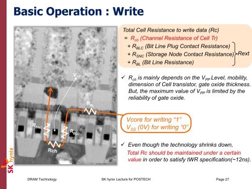
Basic Operation : Write<br />
V PP<br />
Total Cell Resistance to write data (Rc)<br />
= R ch (Channel Resistance of Cell Tr)<br />
+ R BLC (Bit Line Plug Contact Resistance)<br />
+ R SNC (Storage Node Contact Resistance)<br />
+ R BL (Bit Line Resistance)<br />
Vcore for writing “1”<br />
V SS (0V) for writing “0”<br />
Even though the technology shrinks down,<br />
Rext<br />
R ch is mainly depends on the V PP Level, mobility,<br />
dimension of Cell transistor, gate oxide thickness.<br />
But, the maximum value of V PP is limited by the<br />
reliability of gate oxide.<br />
Total Rc should be maintained under a certain<br />
value in order to satisfy tWR specification(~12ns).<br />
<strong>DRAM</strong> <strong>Technology</strong> SK hynix Lecture for POSTECH<br />
Page 27