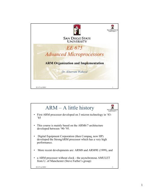
EE 675 Advanced Microprocessors ARM – A little history
EE 675 Advanced Microprocessors ARM – A little history
EE 675 Advanced Microprocessors ARM – A little history

You also want an ePaper? Increase the reach of your titles
YUMPU automatically turns print PDFs into web optimized ePapers that Google loves.
<strong>EE</strong> <strong>675</strong><br />
<strong>Advanced</strong> <strong>Microprocessors</strong><br />
<strong>ARM</strong> Organization and Implementation<br />
Dr. Khurram Waheed<br />
<strong>EE</strong> <strong>675</strong> @ SDSU 1<br />
<strong>ARM</strong> <strong>–</strong> A <strong>little</strong> <strong>history</strong><br />
• First <strong>ARM</strong> processor developed on 3 micron technology in ‘83-<br />
’85<br />
• This course is mainly based on the <strong>ARM</strong>6/7 architecture<br />
developed between ‘90-’95.<br />
• Digital Equipment Corporation (then Compaq, now HP)<br />
developed the Strong<strong>ARM</strong> processor which has a very high<br />
performance.<br />
• More recent developments are: <strong>ARM</strong>8 and <strong>ARM</strong>9E (1999), and<br />
• a <strong>ARM</strong> processor without clock - the asynchronous AMULET<br />
from U. of Manchester (Steve Furber’s group)<br />
<strong>EE</strong> <strong>675</strong> @ SDSU 2<br />
1
<strong>ARM</strong> organization<br />
• Two main blocks: datapath and<br />
decoder<br />
• Register bank<br />
<strong>–</strong> r0 to r15<br />
<strong>–</strong> 2 read ports,<br />
<strong>–</strong> 1 write port<br />
<strong>–</strong> 1 read, 1 write port reserved for r15 (pc)<br />
• Barrel shifter <strong>–</strong> shift or rotate one<br />
operand for any number of bits<br />
• ALU <strong>–</strong> performs the arithmetic and<br />
logic functions required<br />
• Memory address register +<br />
incrementer<br />
• Memory data registers<br />
• Instruction decoder and associated<br />
control logic<br />
address register<br />
register<br />
bank<br />
incrementer<br />
multiply<br />
register<br />
barrel<br />
shifter<br />
data out register<br />
instruction<br />
decode<br />
&<br />
control<br />
D[31:0]<br />
<strong>EE</strong> <strong>675</strong> @ SDSU 3<br />
A<br />
L<br />
U<br />
b<br />
u<br />
s<br />
A[31:0]<br />
<strong>ARM</strong> <strong>–</strong> Internal Organization<br />
3-stage Pipeline<br />
• Data register holds read/write data<br />
from/to memory<br />
• Instruction decoder decodes<br />
machine code instructions to<br />
produce control signals to datapath<br />
• Data processing instructions take a<br />
single cycle: data values are read on<br />
the A-bus & B-bus, the results from<br />
ALU is written back into register<br />
bank<br />
P<br />
C<br />
A<br />
b<br />
u<br />
s<br />
ALU<br />
address register<br />
register<br />
bank<br />
incrementer<br />
multiply<br />
register<br />
barrel<br />
shifter<br />
data out register<br />
PC<br />
B<br />
b<br />
u<br />
s<br />
control<br />
data in register<br />
instruction<br />
decode<br />
&<br />
control<br />
D[31:0]<br />
<strong>EE</strong> <strong>675</strong> @ SDSU 4<br />
A<br />
L<br />
U<br />
b<br />
u<br />
s<br />
A[31:0]<br />
P<br />
C<br />
A<br />
b<br />
u<br />
s<br />
ALU<br />
PC<br />
B<br />
b<br />
u<br />
s<br />
control<br />
data in register<br />
2
Pipelining<br />
• The maximum processing rate is determined by the propagation<br />
delay of the computational logic <strong>–</strong> in abstract:<br />
Function 1 Function 2<br />
Time T1 Time T2<br />
• Above we can process one input every T1+T2<br />
a register<br />
Function 1 Function 2<br />
Time T1 Time T2<br />
• Above we can process one input every max{T1,T2}, but each<br />
input still takes T1+T2 to be completely processed<br />
<strong>EE</strong> <strong>675</strong> @ SDSU 5<br />
Three-stage pipeline<br />
• <strong>ARM</strong> uses a 3-stage instruction pipeline<br />
<strong>–</strong> Fetch: fetch instruction code from memory into the instruction pipeline<br />
<strong>–</strong> Decode: instruction decoded to obtain control signals for the datapath ready<br />
for the next stage<br />
<strong>–</strong> Execute: instruction “owns” the datapath - register read; shifting; ALU results<br />
generated and write-back<br />
• Results for each stage stored in registers<br />
• The consequence is that the clock period is much shorter than without<br />
pipelining<br />
<strong>EE</strong> <strong>675</strong> @ SDSU 6<br />
3
Pipeline: how it works<br />
• All instructions occupy the datapath for one or more<br />
adjacent cycles<br />
• For each cycle that an instruction occupies the datapath,<br />
it occupies the decode logic in the immediately<br />
preceding cycle<br />
• During the first datapath cycle each instruction issues<br />
a fetch for the next instruction but one<br />
• Branch instruction flush and refill the instruction<br />
pipeline<br />
<strong>EE</strong> <strong>675</strong> @ SDSU 7<br />
<strong>ARM</strong> single-cycle instruction<br />
pipeline<br />
1<br />
2<br />
3<br />
instruction<br />
fetch decode execute<br />
fetch decode execute<br />
fetch decode execute<br />
time<br />
• At any time, 3 different instructions may occupy each of the 3-stages of<br />
pipeline<br />
• It may take three cycles to complete a single-cycle instruction. This is<br />
said to have a three cycle latency<br />
• Once a pipeline fills, the processor completes a single-cycle instruction<br />
every clock cycle. Therefore the throughput is one instruction per<br />
cycle.<br />
<strong>EE</strong> <strong>675</strong> @ SDSU 8<br />
4
<strong>ARM</strong> single-cycle instruction<br />
pipeline<br />
fetch<br />
sub r2,r3,r6<br />
cmp r2,#3<br />
decode<br />
fetch<br />
execute add<br />
decode<br />
fetch<br />
1 2 3<br />
add r0,r1,#5<br />
execute sub<br />
decode execute cmp<br />
time<br />
<strong>EE</strong> <strong>675</strong> @ SDSU 9<br />
1<br />
2<br />
3<br />
4<br />
<strong>ARM</strong> multi-cycle instruction<br />
pipeline<br />
fetch ADD decode execute<br />
fetch STR decode calc. addr.<br />
Decode logic is always generating<br />
the control signals for the datapath<br />
to use in the next cycle<br />
data xfer<br />
fetch ADD decode execute<br />
fetch ADD decode execute<br />
5<br />
instruction<br />
fetch ADD<br />
time<br />
decode execute<br />
<strong>EE</strong> <strong>675</strong> @ SDSU 10<br />
5
PC behavior <strong>–</strong> Pipeline<br />
• As a consequence of pipeline, the PC (r15) needs to run<br />
ahead of current instruction<br />
• Instruction fetches the next instruction but one during<br />
their first cycle, i.e., PC points 8 bytes ahead of current<br />
instruction.<br />
• So a user using the PC in a program must account for the<br />
pipeline effects<br />
• The situation is more complex in cycles later than the<br />
first cycle.<br />
<strong>EE</strong> <strong>675</strong> @ SDSU 11<br />
<strong>ARM</strong> multi-cycle LDMIA (load<br />
multiple) instruction<br />
ldmia<br />
r0,{r2,r3}<br />
sub r2,r3,r6<br />
cmp r2,#3<br />
Instruction delayed<br />
fetch decode ex ld r2 ex ld r3<br />
fetch<br />
decode ex sub<br />
Decode stage occupied<br />
since ldmia must continue to<br />
remember decoded instruction<br />
fetch decode ex cmp<br />
time<br />
sub fetched at normal time but<br />
not decoded until LDMIA is finishing<br />
<strong>EE</strong> <strong>675</strong> @ SDSU 12<br />
6
Control stalls: due to branches<br />
• Branches often introduce stalls (branch penalty)<br />
<strong>–</strong> Stall time may depend on whether branch is taken<br />
• May have to squash instructions that already<br />
started executing<br />
• Don’t know what to fetch until condition is<br />
evaluated<br />
<strong>EE</strong> <strong>675</strong> @ SDSU 13<br />
bne foo<br />
sub<br />
r2,r3,r6<br />
foo add<br />
r0,r1,r2<br />
<strong>ARM</strong> pipelined branch<br />
Decision not made until the third clock cycle<br />
fetch decode ex bne<br />
fetch decode<br />
ex bne<br />
ex bne<br />
Two cycles of work thrown<br />
away if bne takes place<br />
fetch decode ex add<br />
time<br />
<strong>EE</strong> <strong>675</strong> @ SDSU 14<br />
7
Expanding the pipeline<br />
• 3-stage pipeline till <strong>ARM</strong>7 is very cost-effective<br />
• Better pipeline architectures required for better<br />
performance<br />
Ninst × CPI<br />
T =<br />
inst<br />
f<br />
• N inst is constant<br />
• So, only two options<br />
<strong>–</strong> Increase the clock rate, f clk requires more pipeline stages<br />
and simpler logic per stage<br />
<strong>–</strong> Reduce the average number of clock cycles per instruction,<br />
CPI requires instructions to occupy fewer pipeline slots and<br />
reduce the stalls in the pipeline Memory Bandwidth<br />
Bottlenecks<br />
clk<br />
<strong>EE</strong> <strong>675</strong> @ SDSU 15<br />
5-stage Pipeline<br />
• Measures to take care of memory bottlenecks<br />
<strong>–</strong> Use of separate code and data memories<br />
<strong>–</strong> Increase the stages in the pipeline reduces the<br />
processor load/clock cycle<br />
• The above steps allow a RISC processor to work<br />
at a higher clock rate.<br />
• Use of separate instruction and data caches<br />
connected to a single DRAM greatly reduces<br />
core’s CPI<br />
<strong>EE</strong> <strong>675</strong> @ SDSU 16<br />
8
<strong>ARM</strong>9TDMI: 5-stage pipeline<br />
• Fetch<br />
• Decode<br />
<strong>–</strong> instruction is decoded<br />
<strong>–</strong> register operands read<br />
(3 read ports)<br />
• Execute<br />
<strong>–</strong> an operand is shifted and the<br />
ALU result generated, or<br />
<strong>–</strong> address is computed<br />
• Buffer/data<br />
<strong>–</strong> data memory is accessed (load,<br />
store)<br />
• Write-back<br />
<strong>–</strong> write to register file<br />
next<br />
pc<br />
pc + 4<br />
B, BL<br />
MOV pc<br />
SUBS pc<br />
LDR pc<br />
register write write-back<br />
<strong>EE</strong> <strong>675</strong> @ SDSU 17<br />
+4<br />
pc+ 8<br />
LDM/<br />
STM post-<br />
+4 index<br />
pre-index<br />
mux<br />
load/store<br />
address<br />
r15<br />
ALU<br />
I-cache<br />
I decode<br />
register read<br />
<strong>ARM</strong>9TDMI: Data Forwarding<br />
ADD r3, r2, r1, LSL #3<br />
ADD r5, r5, r3, LSL r2<br />
ADD r3, r2, r1, LSL #3<br />
ADD r8, r9, r10<br />
ADD r5, r5, r3, LSL r2<br />
LD r3, [r2]<br />
ADD r1, r2, r3<br />
Data Forwarding<br />
Stall?<br />
r3 := r2 + 8 x r1<br />
r5 := r5 + 2 r2 x r3<br />
r3 := r2 + 8 x r1<br />
r8 := r9 + r10<br />
r5 := r5 + 2 r2 x r3<br />
r3 := mem[r2]<br />
r1 := r2 + r3<br />
next<br />
pc<br />
pc + 4<br />
B, BL<br />
MOV pc<br />
SUBS pc<br />
LDR pc<br />
mul<br />
shift<br />
I-cache<br />
reg<br />
shift<br />
byte repl.<br />
D-cache<br />
rot/sgn ex<br />
rot/sgn ex<br />
fetch<br />
instruction<br />
decode<br />
immediate<br />
fields<br />
forwarding<br />
paths<br />
execute<br />
buffer/<br />
data<br />
register write write-back<br />
<strong>EE</strong> <strong>675</strong> @ SDSU 18<br />
+4<br />
pc+8<br />
LDM/<br />
STM post-<br />
+4 index<br />
pre-index<br />
mux<br />
load/store<br />
address<br />
r15<br />
ALU<br />
I decode<br />
register read<br />
mul<br />
shift<br />
reg<br />
shift<br />
byte repl.<br />
D-cache<br />
fetch<br />
instruction<br />
decode<br />
immediate<br />
fields<br />
forwarding<br />
paths<br />
execute<br />
buffer/<br />
data<br />
9
<strong>ARM</strong>9TDMI: PC generation<br />
• 3-stage pipeline<br />
<strong>–</strong> PC behavior:<br />
operands are read in execution<br />
stage<br />
r15 = PC + 8<br />
• 5-stage pipeline<br />
<strong>–</strong> operands are read in decode<br />
stage and r15 = PC + 4?<br />
<strong>–</strong> incompatibilities between 3stage<br />
and 5-stage<br />
implementations =><br />
unacceptable<br />
<strong>–</strong> to avoid this 5-stage pipeline<br />
<strong>ARM</strong>s emulate the behavior of<br />
the older 3-stage designs<br />
next<br />
pc<br />
pc + 4<br />
B, BL<br />
MOV pc<br />
SUBS pc<br />
LDR pc<br />
register write write-back<br />
<strong>EE</strong> <strong>675</strong> @ SDSU 19<br />
+4<br />
pc+ 8<br />
LDM/<br />
STM post-<br />
+4 index<br />
pre-index<br />
mux<br />
load/store<br />
address<br />
r15<br />
ALU<br />
I-cache<br />
I decode<br />
register read<br />
Data processing instruction<br />
datapath activity (Ex)<br />
• Reg-Reg<br />
<strong>–</strong> Rd = Rnop Rm<br />
<strong>–</strong> r15 = AR + 4<br />
AR = AR + 4<br />
• Reg-Imm<br />
<strong>–</strong> Rd = Rnop Imm<br />
<strong>–</strong> r15 = AR + 4<br />
AR = AR + 4<br />
address register<br />
increment<br />
Rd<br />
PC<br />
registers<br />
Rn<br />
Rm<br />
mult<br />
as instruction<br />
as ins.<br />
data out data in i. pipe<br />
(a) register <strong>–</strong> register operations<br />
mul<br />
shift<br />
reg<br />
shift<br />
byte repl.<br />
D-cache<br />
rot/sgn ex<br />
address register<br />
fetch<br />
instruction<br />
decode<br />
immediate<br />
fields<br />
forwarding<br />
paths<br />
increment<br />
Rd<br />
PC<br />
registers<br />
Rn<br />
<strong>EE</strong> <strong>675</strong> @ SDSU 20<br />
mult<br />
as instruction<br />
as ins.<br />
[7:0]<br />
data out data in i. pipe<br />
execute<br />
buffer/<br />
data<br />
(b) register <strong>–</strong> immediate operations<br />
10
STR (store register) datapath<br />
activity (Ex1, Ex2)<br />
• Compute address<br />
(Ex1)<br />
<strong>–</strong> AR = Rn op Disp<br />
<strong>–</strong> r15 = AR + 4<br />
• Store data (Ex2)<br />
<strong>–</strong> AR = PC<br />
<strong>–</strong> mem[AR] =<br />
Rd<br />
<strong>–</strong> If autoindexing<br />
=><br />
Rn = Rn +/- 4<br />
address register<br />
registers<br />
Rn<br />
mult<br />
increment<br />
<strong>EE</strong> <strong>675</strong> @ SDSU 21<br />
lsl #0<br />
= A / A + B / A - B<br />
PC<br />
[11:0]<br />
data out data in i. pipe<br />
Rn<br />
address register<br />
PC<br />
registers<br />
mult<br />
increment<br />
Rd<br />
shifter<br />
= A+ B / A-B<br />
byte? data in i. pipe<br />
(a) 1 st cycle <strong>–</strong> compute address (b) 2 nd cycle <strong>–</strong> store data & auto-index<br />
The first two (of three) cycles of a<br />
branch instruction<br />
• Compute target<br />
address<br />
<strong>–</strong> AR = PC + Disp,lsl #2<br />
• Save return address<br />
(if required)<br />
<strong>–</strong> r14 = PC<br />
<strong>–</strong> AR = AR+ 4<br />
address register<br />
registers<br />
PC<br />
increment<br />
<strong>EE</strong> <strong>675</strong> @ SDSU 22<br />
mult<br />
lsl #2<br />
address register<br />
R14<br />
registers<br />
PC<br />
increment<br />
= A + B<br />
= A<br />
[23:0]<br />
data out data in i. pipe data out data in i. pipe<br />
(a) 1st cycle <strong>–</strong> compute branch target (b) 2nd Third cycle: do a small<br />
correction to the value<br />
stored in the link register in<br />
order that it points to<br />
directly at the instruction<br />
which follows the branch?<br />
cycle <strong>–</strong> save return address<br />
mult<br />
shifter<br />
11
• Datapath<br />
<strong>ARM</strong> Implementation<br />
<strong>–</strong> RTL (Register Transfer Level) description<br />
• Control unit<br />
<strong>–</strong> FSM (Finite State Machine) description<br />
<strong>EE</strong> <strong>675</strong> @ SDSU 23<br />
2-phase non-overlapping clock<br />
scheme<br />
• Most <strong>ARM</strong>s do not operate on edge-sensitive registers<br />
• Instead the design is based around 2-phase non-overlapping clocks<br />
which are generated internally from a single clock signal<br />
• Data movement is controlled by passing the data alternatively<br />
through latches which are open during phase 1 or latches during<br />
phase 2<br />
phase 1<br />
1 clock cycle<br />
phase 2<br />
<strong>EE</strong> <strong>675</strong> @ SDSU 24<br />
12
<strong>ARM</strong> datapath timing<br />
• Register read<br />
<strong>–</strong> Register read buses -- dynamic, precharged during phase 2<br />
<strong>–</strong> During phase 1 selected registers discharge the read buses<br />
which become valid early in phase 1<br />
• Shift operation<br />
<strong>–</strong> second operand passes through barrel shifter<br />
• ALU operation<br />
<strong>–</strong> ALU has input latches which are open in phase 1,<br />
allowing the operands to begin combining in ALU<br />
as soon as they are valid, but they close at the end of phase 1<br />
so that the phase 2 precharge does not get through to the ALU<br />
<strong>–</strong> ALU processes the operands during the phase 2, producing the<br />
valid output towards the end of the phase<br />
<strong>–</strong> the result is latched in the destination register<br />
at the end of phase 2<br />
<strong>EE</strong> <strong>675</strong> @ SDSU 25<br />
<strong>ARM</strong> datapath timing (cont’d)<br />
register<br />
read<br />
time<br />
shift time<br />
phase 1<br />
read bus valid<br />
ALU operands<br />
latched<br />
shift out valid<br />
ALU time<br />
phase 2<br />
precharge<br />
invalidates<br />
buses<br />
register<br />
write time<br />
ALU out<br />
Minimum Datapath Delay = Register read time + Shifter Delay + ALU Delay<br />
+ Register write set-up time<br />
+ Phase 2 to phase 1 non-overlap time<br />
<strong>EE</strong> <strong>675</strong> @ SDSU 26<br />
13
The original <strong>ARM</strong>1 ripple-carry<br />
adder<br />
• Carry logic: use CMOS AOI (And-Or-Invert) gate<br />
• Even bits use circuit show below<br />
• Odd bits use the dual circuit with inverted inputs and<br />
outputs and AND and OR gates swapped around<br />
• Worst case path: 32 gates long<br />
A<br />
B<br />
Cin<br />
<strong>EE</strong> <strong>675</strong> @ SDSU 27<br />
Cin[0]<br />
<strong>EE</strong> <strong>675</strong> @ SDSU 28<br />
Cout<br />
<strong>ARM</strong>2 4-bit carry look-ahead<br />
scheme<br />
• Carry Generate (G)<br />
Carry Propagate (P)<br />
• Cout[3] =Cin[0].P + G<br />
• Use AOI and alternate AND/OR gates<br />
• Worst case: 8 gates long<br />
A[3:0]<br />
B[3:0]<br />
G<br />
P<br />
Cout[3]<br />
4-bit<br />
adder<br />
logic<br />
sum<br />
sum[3:0]<br />
14
The <strong>ARM</strong>2 ALU logic for one<br />
result bit<br />
• ALU functions<br />
<strong>–</strong> data operations (add, sub, ...)<br />
<strong>–</strong> address computations for memory accesses<br />
<strong>–</strong> branch target computations<br />
fs:<br />
<strong>–</strong> bit-wise logical<br />
NB<br />
operations<br />
bus<br />
5 0 1 2 3<br />
carry<br />
logic<br />
G<br />
4<br />
<strong>–</strong> ... ALU<br />
NA<br />
bus<br />
<strong>EE</strong> <strong>675</strong> @ SDSU 29<br />
<strong>ARM</strong>2 ALU function codes<br />
fs5 fs4 fs3 fs2 fs1 fs0 ALU output<br />
0 0 0 1 0 0 A and B<br />
0 0 1 0 0 0 A and not B<br />
0 0 1 0 0 1 A xor B<br />
0 1 1 0 0 1 A plus not B plus carry<br />
0 1 0 1 1 0 A plus B plus carry<br />
1 1 0 1 1 0 not A plus B plus carry<br />
0 0 0 0 0 0 A<br />
0 0 0 0 0 1 A or B<br />
0 0 0 1 0 1 B<br />
0 0 1 0 1 0 not B<br />
0 0 1 1 0 0 zero<br />
<strong>EE</strong> <strong>675</strong> @ SDSU 30<br />
P<br />
bus<br />
15
The <strong>ARM</strong>6 carry-select adder<br />
scheme<br />
• Compute sums of<br />
various fields of<br />
the word<br />
for carry-in of zero<br />
and carry-in of one<br />
• Final result is<br />
selected by using<br />
the correct carry-in<br />
value to control a<br />
multiplexer<br />
a,b[3:0]<br />
sum[3:0] sum[7:4]<br />
Worst case:<br />
O(log 2 [word width]) gates long<br />
+ +, +1 +, +1<br />
c s s+1<br />
mux<br />
sum[15:8]<br />
sum[31:16]<br />
a,b[31:28]<br />
<strong>EE</strong> <strong>675</strong> @ SDSU 31<br />
mux<br />
mux<br />
Note: Be careful! Fan-out on some of these<br />
gates is high so direct comparison with previous<br />
schemes is not applicable.<br />
The <strong>ARM</strong>6 ALU organization<br />
• Not easy to merge the arithmetic and logic<br />
functions =>a separate logic unit runs in parallel<br />
with the adder, and multiplexor selects the output<br />
invert A<br />
function<br />
logic/arithmetic<br />
A operand latch B operand latch<br />
XOR gates XOR gates<br />
logic functions<br />
result mux<br />
zero detect<br />
adder<br />
invert B<br />
C in<br />
C<br />
V<br />
result<br />
<strong>EE</strong> <strong>675</strong> @ SDSU 32<br />
N<br />
Z<br />
16
<strong>ARM</strong>9 carry arbitration encoding<br />
• Carry arbitration adder<br />
ai bi Ci vi, wi<br />
0<br />
1<br />
1<br />
0<br />
v<br />
i<br />
w<br />
i<br />
0<br />
1<br />
0<br />
1<br />
= a<br />
i<br />
i<br />
0<br />
1<br />
u<br />
u<br />
+ b<br />
= a ⋅ b<br />
i<br />
i<br />
0, 0<br />
1, 1<br />
1, 0<br />
1, 0<br />
ai<br />
0<br />
1<br />
0(1)<br />
0(1)<br />
0(1)<br />
1(0)<br />
1(0)<br />
1(0)<br />
0(1)<br />
1(0)<br />
<strong>EE</strong> <strong>675</strong> @ SDSU 33<br />
bi<br />
0<br />
1<br />
ai-1<br />
-<br />
-<br />
0<br />
1<br />
bi-1<br />
-<br />
-<br />
0<br />
1<br />
Ci<br />
0<br />
1<br />
0<br />
1<br />
u<br />
vi, wi<br />
The cross-bar switch barrel shifter<br />
• Shifter delay is critical since it contributes<br />
directly to the datapath cycle time<br />
• Cross-bar switch matrix (32 x 32)<br />
• Principle for 4x4 matrix<br />
in[3]<br />
in[2]<br />
in[1]<br />
in[0]<br />
right 3right<br />
2 right 1<br />
out[0] out[1] out[2] out[3]<br />
no shift<br />
<strong>EE</strong> <strong>675</strong> @ SDSU 34<br />
left 1<br />
left 2<br />
left 3<br />
0, 0<br />
1, 1<br />
0, 0<br />
1, 1<br />
1, 0<br />
17
The cross-bar switch barrel shifter<br />
(cont’d)<br />
• Precharged logic is used => each switch is a single NMOS<br />
transistor<br />
• Precharging sets all outputs to logic 0, so those which are not<br />
connected to any input during switching remain at 0 giving the zero<br />
filling required by the shift semantics<br />
• For rotate right, the right shift diagonal is enabled + complementary<br />
shift left diagonal (e. g., ‘right 1’ + ‘left 3’)<br />
• Arithmetic shift right: use sign-extension => separate logic is used<br />
to decode the shift amount and discharge those outputs<br />
appropriately<br />
<strong>EE</strong> <strong>675</strong> @ SDSU 35<br />
Multiplier design<br />
• All <strong>ARM</strong>s apart form the first prototype have included<br />
support for integer multiplication<br />
<strong>–</strong> older <strong>ARM</strong> cores include low-cost multiplication hardware<br />
that supports only the 32-bit result multiply and<br />
multiply-accumulate<br />
<strong>–</strong> recent <strong>ARM</strong> cores have high-performance multiplication<br />
hardware and support 64-bit result multiply and<br />
multiply-accumulate<br />
• Low cost implementation<br />
<strong>–</strong> Use the datapath iteratively, employing the barrel shifter<br />
and ALU to generate 2-bit product in each clock cycle<br />
<strong>–</strong> use early termination to stop the iterations when there are no<br />
more ones in the multiply register<br />
<strong>EE</strong> <strong>675</strong> @ SDSU 36<br />
18
The 2-bit multiplication<br />
algorithm, Nth cycle<br />
• Control settings for the Nth cycle of the multiplication<br />
• Use existing shifter and ALU + additional hardware<br />
<strong>–</strong> dedicated two-bits-per-cycle shift register for the multiplier and<br />
a few gates for the Booth’s algorithm control logic<br />
(overhead is a few per cent on the area of <strong>ARM</strong> core)<br />
Carry-in Multiplier Shift ALU Carry-out<br />
0 x0 LSL#2N A+0 0<br />
x1 LSL#2N A+B 0<br />
x2 LSL#(2N+1) A<strong>–</strong> B 1<br />
x3 LSL#2N A<strong>–</strong> B 1<br />
1 x0 LSL#2N A+B 0<br />
x1 LSL#(2N+1) A+B 0<br />
x2 LSL#2N A<strong>–</strong> B 1<br />
x3 LSL#2N A+0 1<br />
<strong>EE</strong> <strong>675</strong> @ SDSU 37<br />
High speed multiplication<br />
• Where multiplication performance is very important,<br />
more hardware resources must be dedicated<br />
<strong>–</strong> in some embedded systems the <strong>ARM</strong> core is used to perform<br />
real-time digital signal processing (DSP) <strong>–</strong><br />
DSP programs are typically multiplication intensive<br />
• Use intermediate results which include<br />
partial sums and partial carries<br />
<strong>–</strong> Carry-save adders are used for this<br />
• These two binary results are added together at the end of<br />
multiplication<br />
<strong>–</strong> The main ALU is used for this<br />
<strong>EE</strong> <strong>675</strong> @ SDSU 38<br />
19
Carry-propagate (a) and carrysave<br />
(b) adder structures<br />
• Carry propagate adder takes two conventional (irredundant) binary<br />
numbers as inputs and produces a binary sum<br />
• Carry save adder takes one binary and one redundant (partial sum<br />
and partial carry) input and produces a sum in redundant binary<br />
representation (sum and carry)<br />
A B Cin A B Cin<br />
(a) +<br />
+<br />
Cout S Cout S<br />
A B Cin A B Cin<br />
(b) +<br />
+<br />
Cout S Cout S<br />
A B Cin<br />
+<br />
Cout S<br />
A B Cin<br />
+<br />
Cout S<br />
A B Cin<br />
+<br />
Cout S<br />
A B Cin<br />
+<br />
Cout S<br />
<strong>EE</strong> <strong>675</strong> @ SDSU 39<br />
<strong>ARM</strong> high-speed multiplier<br />
organization<br />
• CSA has 4 layers of adders each handling 2 multiplier bits =><br />
multiply 8-bits per clock cycle<br />
• Partial sum and carry are cleared at the beginning or initialized to<br />
accumulate a value<br />
• Multiplier is shifted right 8-bits per cycle in the ‘Rs’ register<br />
• Carry sum and carry are rotated right 8 bits per cycle<br />
• Performance: up to 4 clock cycles (early termination is possible)<br />
• Complexity: 160 bits in shift registers, 128 bits of carry-save<br />
adder logic (up to 10% of simpler cores)<br />
<strong>EE</strong> <strong>675</strong> @ SDSU 40<br />
20
<strong>ARM</strong> high-speed multiplier<br />
organization<br />
initialization for MLA<br />
rotate sum and<br />
carry 8 bits/cycle<br />
partial sum<br />
partial carry<br />
registers<br />
Rs >> 8 bits/cycle<br />
carry-save adders<br />
<strong>EE</strong> <strong>675</strong> @ SDSU 41<br />
Rm<br />
ALU (add partials)<br />
<strong>ARM</strong>2 register cell circuit<br />
• Asymmetric cross-coupled pair of MOS inverters<br />
• Feedback inverter is weak to minimize resistance to new<br />
value for the register<br />
• Newer cores use the complementary MOS technology<br />
ALU bus<br />
A bus<br />
B bus<br />
write<br />
read<br />
A<br />
Register cell structure upto <strong>ARM</strong>6<br />
read<br />
B<br />
<strong>EE</strong> <strong>675</strong> @ SDSU 42<br />
21
<strong>ARM</strong> register bank floorplan<br />
• Enable lines run vertically and data busses run horizontally<br />
• Decoders are more complex that the register cells but horizontal<br />
pitch is matched to register cells<br />
Vdd<br />
Vss<br />
ALU<br />
bus<br />
PC<br />
bus<br />
INC<br />
bus<br />
PC<br />
A bus read decoders<br />
B bus read decoders<br />
write decoders<br />
register cells<br />
ALU<br />
bus<br />
A bus<br />
B bus<br />
<strong>EE</strong> <strong>675</strong> @ SDSU 43<br />
<strong>ARM</strong> core datapath buses<br />
• Datapath pitch is chosen as a compromise between the complex<br />
functions (ALU) and simpler functions (barrel shifter)<br />
• Space is also allocated for the passage of passenger buses<br />
Ad<br />
PC inc<br />
shift out<br />
W<br />
instruction<br />
Din<br />
A B<br />
address register<br />
incrementer<br />
register bank<br />
multiplier<br />
ALU<br />
shifter<br />
data in<br />
instruction pipe<br />
data out<br />
<strong>EE</strong> <strong>675</strong> @ SDSU 44<br />
22
<strong>ARM</strong> control logic structure<br />
• Three structural components<br />
<strong>–</strong> Instruction decoder PLA: uses some instruction bits<br />
and an internal cycle counter to define the class of<br />
operation during the next cycle<br />
<strong>–</strong> Distributed Secondary Control: selects other<br />
instruction bits and/or processor state information to<br />
control the datapath<br />
<strong>–</strong> Decentralized Control Units: for specific instructions<br />
that take a variable number of cycles to complete<br />
(load/store, multiply, coprocessor etc.)<br />
<strong>EE</strong> <strong>675</strong> @ SDSU 45<br />
<strong>ARM</strong> control logic structure<br />
address<br />
control<br />
decode<br />
PLA<br />
register<br />
control<br />
instruction<br />
cycle<br />
count<br />
ALU<br />
control<br />
coprocessor<br />
multiply<br />
control<br />
load/store<br />
multiple<br />
shifter<br />
control<br />
<strong>EE</strong> <strong>675</strong> @ SDSU 46<br />
23