Analog CMOS Integrated Circuit Design Set 2 - Courses - University ...
Analog CMOS Integrated Circuit Design Set 2 - Courses - University ...
Analog CMOS Integrated Circuit Design Set 2 - Courses - University ...

You also want an ePaper? Increase the reach of your titles
YUMPU automatically turns print PDFs into web optimized ePapers that Google loves.
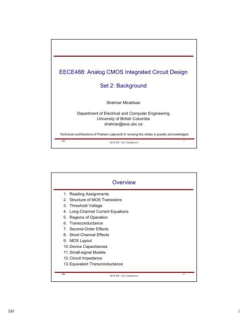
EECE488: <strong>Analog</strong> <strong>CMOS</strong> <strong>Integrated</strong> <strong>Circuit</strong> <strong>Design</strong><br />
SM<br />
<strong>Set</strong> 2: Background<br />
Shahriar Mirabbasi<br />
Department of Electrical and Computer Engineering<br />
<strong>University</strong> of British Columbia<br />
shahriar@ece.ubc.ca<br />
Technical contributions of Pedram Lajevardi in revising the slides is greatly acknowledged.<br />
SM<br />
EECE 488 – <strong>Set</strong> 2: Background<br />
Overview<br />
1. Reading Assignments<br />
2. Structure of MOS Transistors<br />
3. Threshold Voltage<br />
4. Long-Channel Current Equations<br />
5. Regions of Operation<br />
6. Transconductance<br />
7. Second-Order Effects<br />
8. Short-Channel Effects<br />
9. MOS Layout<br />
10.Device Capacitances<br />
11.Small-signal Models<br />
12.<strong>Circuit</strong> Impedance<br />
13.Equivalent Transconductance<br />
EECE 488 – <strong>Set</strong> 2: Background<br />
SM 1<br />
1<br />
2
• Reading:<br />
SM<br />
Chapter 2 of the textbook<br />
Section 16.2 of the textbook<br />
Chapter 17<br />
Reading Assignments<br />
All the figures in the lecture notes are © <strong>Design</strong> of <strong>Analog</strong> <strong>CMOS</strong> <strong>Integrated</strong> <strong>Circuit</strong>s,<br />
McGraw-Hill, 2001, unless otherwise noted.<br />
• Transistor stands for …<br />
SM<br />
EECE 488 – <strong>Set</strong> 2: Background<br />
Transistor<br />
• Transistor are semiconductor devices that can be classified as<br />
– Bipolar Junction Transistors (BJTs)<br />
– Field Effect Transistors (FETs)<br />
• Depletion-Mode FETs or (e.g., JFETs)<br />
• Enhancement-Mode FETs (e.g., MOSFETs)<br />
EECE 488 – <strong>Set</strong> 2: Background<br />
SM 2<br />
3<br />
4
SM<br />
Simplistic Model<br />
• MOS transistors have three terminals: Gate, Source, and Drain<br />
• The voltage of the Gate terminal determines the type of connection<br />
between Source and Drain (Short or Open).<br />
• Thus, MOS devices behave like a switch<br />
SM<br />
V G high<br />
V G low<br />
NMOS<br />
Device is ON<br />
D is shorted to S<br />
Device is OFF<br />
D & S are disconnected<br />
EECE 488 – <strong>Set</strong> 2: Background<br />
Device is OFF<br />
D & S are disconnected<br />
Device is ON<br />
D is shorted to S<br />
Physical Structure - 1<br />
SM 3<br />
PMOS<br />
• Source and Drain terminals are identical except that Source provides<br />
charge carriers, and Drain receives them.<br />
• MOS devices have in fact 4 terminals:<br />
– Source, Drain, Gate, Substrate (bulk)<br />
© Microelectronic <strong>Circuit</strong>s, 2004 Oxford <strong>University</strong> Press<br />
EECE 488 – <strong>Set</strong> 2: Background<br />
5<br />
6
SM<br />
Physical Structure - 2<br />
• Charge Carriers are electrons in NMOS devices, and holes in<br />
PMOS devices.<br />
• Electrons have a higher mobility than holes<br />
• So, NMOS devices are faster than PMOS devices<br />
• We rather to have a p-type substrate?!<br />
EECE 488 – <strong>Set</strong> 2: Background<br />
L D: Due to Side Diffusion<br />
Poly-silicon used instead of Metal<br />
for fabrication reasons<br />
• Actual length of the channel (L eff) is less than the length of gate<br />
SM<br />
Physical Structure - 3<br />
• N-wells allow both NMOS and PMOS devices to reside on the<br />
same piece of die.<br />
• As mentioned, NMOS and PMOS devices have 4 terminals:<br />
Source, Drain, Gate, Substrate (bulk)<br />
• In order to have all PN junctions reverse-biased, substrate of<br />
NMOS is connected to the most negative voltage, and substrate<br />
of PMOS is connected to the most positive voltage.<br />
EECE 488 – <strong>Set</strong> 2: Background<br />
SM 4<br />
7<br />
8
• MOS transistor Symbols:<br />
SM<br />
Physical Structure - 4<br />
electron<br />
• In NMOS Devices: Source ⎯⎯⎯→<br />
Drain<br />
Current flows from Drain to Source<br />
• In PMOS Devices:<br />
hole<br />
Source ⎯⎯→<br />
Drain<br />
Current flows from Source to Drain<br />
• Current flow determines which terminal is Source and which one<br />
is Drain. Equivalently, source and drain can be determined based<br />
on their relative voltages.<br />
SM<br />
EECE 488 – <strong>Set</strong> 2: Background<br />
Threshold Voltage - 1<br />
• Consider an NMOS: as the gate voltage is increased, the surface<br />
under the gate is depleted. If the gate voltage increases more,<br />
free electrons appear under the gate and a conductive channel is<br />
formed.<br />
(a) An NMOS driven by a gate voltage, (b) formation of depletion region, (c) onset of inversion,<br />
and (d) channel formation<br />
• As mentioned before, in NMOS devices charge carriers in the<br />
channel under the gate are electrons.<br />
EECE 488 – <strong>Set</strong> 2: Background<br />
SM 5<br />
9<br />
10
SM<br />
Threshold Voltage - 2<br />
• Intuitively, the threshold voltage is the gate voltage that forces the<br />
interface (surface under the gate) to be completely depleted of charge (in<br />
NMOS the interface is as much n-type as the substrate is p-type)<br />
• Increasing gate voltage above this threshold (denoted by V TH or V t)<br />
induces an inversion layer (conductive channel) under the gate.<br />
SM<br />
Analytically:<br />
V TH = Φ MS + 2 ⋅ Φ F<br />
Q<br />
+<br />
C<br />
Where:<br />
= the<br />
© Microelectronic <strong>Circuit</strong>s, 2004 Oxford <strong>University</strong> Press<br />
EECE 488 – <strong>Set</strong> 2: Background<br />
Threshold Voltage - 3<br />
ΦMS = Built - in Potential = Φ gate − ΦSilicon<br />
Φ<br />
F<br />
dep<br />
dep<br />
ox<br />
difference between the work functions of<br />
the polysilicon<br />
gate and the silicon substrate<br />
= Work Function (electrostatic<br />
potential)<br />
EECE 488 – <strong>Set</strong> 2: Background<br />
K ⋅T<br />
⎛ N<br />
⋅ ln⎜<br />
q ⎝ ni<br />
Q = Charge<br />
in the depletion region = 4 ⋅ q ⋅ε<br />
⋅ Φ ⋅ N<br />
SM 6<br />
=<br />
si<br />
F<br />
sub<br />
sub<br />
⎞<br />
⎟<br />
⎠<br />
11<br />
12
SM<br />
Threshold Voltage - 4<br />
• In practice, the “native” threshold value may not be suited for<br />
circuit design, e.g., V TH may be zero and the device may be on for<br />
any positive gate voltage.<br />
• Typically threshold voltage is adjusted by ion implantation into the<br />
channel surface (doping P-type material will increase V TH of<br />
NMOS devices).<br />
• When V DS is zero, there is no horizontal electric field present in the<br />
channel, and therefore no current between the source to the drain.<br />
• When V DS is more than zero, there is some horizontal electric field<br />
which causes a flow of electrons from source to drain.<br />
SM<br />
EECE 488 – <strong>Set</strong> 2: Background<br />
Long Channel Current Equations - 1<br />
• The voltage of the surface under the gate, V(x), depends on the<br />
voltages of Source and Drain.<br />
• If V DS is zero, V D= V S=V(x). The charge density Q d (unit C/m) is uniform.<br />
Q<br />
d<br />
EECE 488 – <strong>Set</strong> 2: Background<br />
− Q − C ⋅V<br />
−<br />
= = =<br />
L L<br />
Q = −WC<br />
−<br />
ox ( VGS<br />
VTH<br />
SM 7<br />
d<br />
Qd ( x)<br />
= −WCox<br />
( VGS<br />
−V<br />
( x)<br />
−VTH<br />
)<br />
)<br />
13<br />
( C WL)<br />
⋅ ( V −V<br />
)<br />
• If V DS is not zero, the channel is tapered, and V(x) is not constant. The<br />
charge density depends on x.<br />
ox<br />
L<br />
GS<br />
TH<br />
14
SM<br />
Long Channel Current Equations - 3<br />
dQ dQ dx<br />
I Qd<br />
velocity<br />
dt dx dt<br />
⋅ = × = =<br />
• Current :<br />
Velocity in terms of V(x):<br />
dV<br />
velocity = μ ⋅ E , E = −<br />
dt<br />
− dV ( x)<br />
→ velocity = ( μ ⋅ )<br />
dx<br />
Qd in terms of V(x):<br />
Qd ( x)<br />
= −WC<br />
ox ( VGS<br />
−V<br />
( x)<br />
−VTH<br />
)<br />
• Current in terms of V(x):<br />
L<br />
∫ I dx = ∫WC<br />
μ [ V<br />
D<br />
x=<br />
0<br />
dV ( x)<br />
= WCox<br />
[ VGS<br />
−V<br />
( x)<br />
−VTH<br />
] μ<br />
dx<br />
I D<br />
n<br />
V<br />
DS<br />
V = 0<br />
• Long-channel current equation:<br />
SM<br />
ox<br />
n<br />
GS<br />
−V<br />
( x)<br />
−V<br />
W<br />
1<br />
I D = μ nC<br />
ox [( VGS<br />
−VTH<br />
) VDS<br />
− V<br />
L<br />
2<br />
EECE 488 – <strong>Set</strong> 2: Background<br />
SM 8<br />
TH<br />
2<br />
DS<br />
© Microelectronic <strong>Circuit</strong>s, 2004 Oxford <strong>University</strong> Press<br />
] dV<br />
Long Channel Current Equations - 4<br />
• If V DS ≤ V GS-V TH we say the device is operating in triode (or linear) region.<br />
• Current in Triode Region:<br />
EECE 488 – <strong>Set</strong> 2: Background<br />
]<br />
I = μ ⋅ C<br />
• Terminology:<br />
W<br />
Aspect Ratio =<br />
L<br />
Overdrive Voltage = Effective<br />
D<br />
n<br />
ox<br />
W ⎡<br />
1 2 ⎤<br />
⋅ ⋅<br />
⎢(<br />
VGS<br />
−VTH<br />
) ⋅VDS<br />
− ⋅VDS<br />
L ⎣<br />
2 ⎥<br />
⎦<br />
Voltage = V<br />
GS<br />
−V<br />
TH<br />
= V<br />
eff<br />
15<br />
16
If V<br />
SM<br />
DS<br />
Long Channel Current Equations - 5<br />
• For very small V DS (deep Triode Region):<br />
I D can be approximated to be a linear function of V DS.<br />
The device resistance will be independent of V DS and will<br />
only depend on V eff.<br />
The device will behave like a variable resistor<br />
SM<br />
I<br />
D<br />
SM<br />
= I<br />
Long Channel Current Equations - 7<br />
• If V DS > V GS – V TH, the transistor is in saturation (active) region,<br />
and the channel is pinched off.<br />
L'<br />
∫ I dx =<br />
D<br />
x=<br />
0<br />
VGS<br />
−VTH<br />
∫WC<br />
μ [ V<br />
V = 0<br />
ox<br />
1 W<br />
I D = μnC<br />
ox ( VGS<br />
−V<br />
2 L'<br />
n<br />
GS<br />
TH<br />
)<br />
−V<br />
( x)<br />
−V<br />
2<br />
TH<br />
EECE 488 – <strong>Set</strong> 2: Background<br />
SM 10<br />
] dV<br />
• Let’s, for now, assume that L’=L. The fact that<br />
L’ is not equal to L is a second-order effect<br />
known as channel-length modulation.<br />
• Since I D only depends on V GS, MOS transistors in saturation can be<br />
used as current sources.<br />
SM<br />
Long Channel Current Equations - 8<br />
• Current Equation for NMOS:<br />
DS<br />
⎧<br />
⎪0<br />
; if VGS<br />
< VTH<br />
( Cut − off )<br />
⎪<br />
⎪<br />
⎪ W<br />
⎪μ<br />
n ⋅ Cox<br />
⋅ ⋅(<br />
VGS<br />
−VTH<br />
) ⋅V<br />
⎪ L<br />
= ⎨<br />
⎪ W<br />
⎪μ<br />
n ⋅ Cox<br />
⋅ ⋅<br />
⎪ L<br />
⎪<br />
⎪<br />
⎪1<br />
W<br />
2<br />
⋅ μ ⋅ C ⋅ ⋅ ( V −V<br />
)<br />
⎪ n ox<br />
GS TH<br />
⎩2<br />
L<br />
DS<br />
; if V<br />
1 2<br />
[ ( VGS<br />
−VTH<br />
) ⋅V<br />
DS − ⋅VDS<br />
]<br />
2<br />
; if V<br />
GS<br />
GS<br />
> V<br />
> V<br />
EECE 488 – <strong>Set</strong> 2: Background<br />
, V<br />
; if V<br />
TH<br />
TH<br />
, V<br />
GS<br />
DS<br />
DS<br />
V<br />
> V<br />
TH<br />
GS<br />
GS<br />
, V<br />
DS<br />
−V<br />
TH<br />
−V<br />
TH<br />
< V<br />
GS<br />
−V<br />
( Saturation )<br />
19<br />
) ( Deep Triode)<br />
TH<br />
( Triode)<br />
20
I<br />
D<br />
SM<br />
Long Channel Current Equations - 9<br />
• Current Equation for PMOS:<br />
= I<br />
SM<br />
SD<br />
⎧<br />
⎪0<br />
; if VSG<br />
< VTH<br />
( Cut − off )<br />
⎪<br />
⎪<br />
⎪ W<br />
⎪μ<br />
p ⋅ Cox<br />
⋅ ⋅(<br />
VSG<br />
− VTH<br />
) ⋅V<br />
⎪ L<br />
= ⎨<br />
⎪ W<br />
⎪μ<br />
p ⋅ Cox<br />
⋅ ⋅<br />
⎪ L<br />
⎪<br />
⎪<br />
⎪1<br />
W<br />
2<br />
⎪<br />
⋅ μ p ⋅ Cox<br />
⋅ ⋅ ( VSG<br />
− VTH<br />
)<br />
⎩2<br />
L<br />
SD<br />
; if V<br />
1 2<br />
[ ( VSG<br />
− VTH<br />
) ⋅VSD<br />
− ⋅VSD<br />
]<br />
2<br />
; if V<br />
EECE 488 – <strong>Set</strong> 2: Background<br />
SM 11<br />
SG<br />
> V<br />
> V<br />
; if V<br />
TH<br />
, V<br />
SG<br />
, V<br />
SD<br />
V<br />
> V<br />
Regions of Operation - 1<br />
SG<br />
TH<br />
SD<br />
TH<br />
SG<br />
SG<br />
, V<br />
SD<br />
− V<br />
• Regions of Operation:<br />
Cut-off, triode (linear), and saturation (active or pinch-off)<br />
© Microelectronic <strong>Circuit</strong>s, 2004 Oxford <strong>University</strong> Press<br />
EECE 488 – <strong>Set</strong> 2: Background<br />
− V<br />
TH<br />
TH<br />
< V<br />
SG<br />
) ( Deep Triode)<br />
− V<br />
TH<br />
( Saturation )<br />
• Once the channel is pinched off, the current through the channel is<br />
almost constant. As a result, the I-V curves have a very small slope in<br />
the pinch-off (saturation) region, indicating the large channel<br />
resistance.<br />
( Triode)<br />
21<br />
22
SM<br />
Regions of Operation - 2<br />
• The following illustrates the transition from pinch-off to triode region for<br />
NMOS and PMOS devices.<br />
• For NMOS devices:<br />
If V D increases (V G Const.), the device will go from Triode to Pinch-off.<br />
If V G increases (V D Const.), the device will go from Pinch-off to Triode.<br />
** In NMOS, as V DG increases the device will go from Triode to Pinch-off.<br />
• For PMOS devices:<br />
If V D decreases (V G Const.), the device will go from Triode to Pinch-off.<br />
If V G decreases (V D Const.), the device will go from Pinch-off to Triode.<br />
** In PMOS, as V GD increases the device will go from Pinch-off to Triode.<br />
• NMOS Regions of Operation:<br />
SM<br />
EECE 488 – <strong>Set</strong> 2: Background<br />
Regions of Operation - 3<br />
© Microelectronic <strong>Circuit</strong>s, 2004 Oxford <strong>University</strong> Press<br />
• Relative levels of the terminal voltages of the enhancement-type NMOS<br />
transistor for different regions of operation.<br />
EECE 488 – <strong>Set</strong> 2: Background<br />
SM 12<br />
23<br />
24
• PMOS Regions of Operation:<br />
SM<br />
Regions of Operation - 4<br />
© Microelectronic <strong>Circuit</strong>s, 2004 Oxford <strong>University</strong> Press<br />
• The relative levels of the terminal voltages of the enhancement-type<br />
PMOS transistor for different regions of operation.<br />
SM<br />
EECE 488 – <strong>Set</strong> 2: Background<br />
Regions of Operation - 5<br />
Example:<br />
For the following circuit assume that V TH=0.7V.<br />
• When is the device on?<br />
• What is the region of operation if the device is on?<br />
• Sketch the on-resistance of transistor M 1 as a function of V G.<br />
EECE 488 – <strong>Set</strong> 2: Background<br />
SM 13<br />
25<br />
26
SM<br />
Transconductance - 1<br />
• The drain current of the MOSFET in saturation region is ideally a<br />
function of gate-overdrive voltage (effective voltage). In reality, it is also<br />
a function of V DS.<br />
• It makes sense to define a figure of merit that indicates how well the<br />
device converts the voltage to current.<br />
• Which current are we talking about?<br />
• What voltage is in the designer’s control?<br />
• What is this figure of merit?<br />
• Transconductance in triode:<br />
SM<br />
g<br />
m<br />
∂I<br />
=<br />
∂V<br />
• Transconductance in saturation:<br />
D<br />
GS<br />
= Const.<br />
EECE 488 – <strong>Set</strong> 2: Background<br />
Transconductance - 2<br />
∂ ⎛ W<br />
g m = ⎜ μ n ⋅C<br />
ox ⋅<br />
∂VGS<br />
⎝ L<br />
W<br />
= μ n ⋅ Cox<br />
⋅ ⋅VDS<br />
L<br />
SM 14<br />
V<br />
Example:<br />
Plot the transconductance of the following circuit as a function of V DS<br />
(assume V b is a constant voltage).<br />
∂ ⎛ W<br />
g m = ⎜ ⋅ μ n ⋅ Cox<br />
⋅ ⋅ ( V<br />
∂VGS<br />
⎝ 2 L<br />
W<br />
= μ n ⋅ Cox<br />
⋅ ⋅ ( VGS<br />
−VTH<br />
)<br />
L<br />
DS<br />
1 2<br />
⋅[<br />
( VGS<br />
−VTH<br />
) ⋅VDS<br />
− ⋅VDS<br />
]<br />
1 2<br />
GS −VTH<br />
)<br />
EECE 488 – <strong>Set</strong> 2: Background<br />
2<br />
⎞<br />
⎟<br />
⎠ V<br />
DS<br />
⎞<br />
⎟<br />
⎠ V<br />
DS<br />
= Const.<br />
= Const.<br />
• Moral: Transconductance drops if the device enters the triode region.<br />
27<br />
28
SM<br />
Transconductance - 3<br />
• Transconductance, gm, in saturation:<br />
W<br />
g m = μ n ⋅ Cox<br />
⋅ ⋅ ( VGS<br />
−VTH<br />
) = 2μ<br />
n ⋅ C<br />
L<br />
EECE 488 – <strong>Set</strong> 2: Background<br />
SM 15<br />
ox<br />
W<br />
⋅ ⋅ I<br />
L<br />
D<br />
2 ⋅ I D<br />
=<br />
V −V<br />
• If the aspect ratio is constant: g m depends linearly on (V GS - V TH).<br />
Also, g m depends on square root of I D.<br />
• If I D is constant: g m is inversely proportional to (V GS - V TH).<br />
Also, g m depends on square root of the aspect ratio.<br />
• If the overdrive voltage is constant: g m depends linearly on I D.<br />
Also, g m depends linearly on the aspect ratio.<br />
SM<br />
Second-Order Effects (Body Effect)<br />
Substrate Voltage:<br />
• So far, we assumed that the bulk and source of the transistor are at the<br />
same voltage (V B=V S).<br />
• If V B >V s, then the bulk-source PN junction will be forward biased, and<br />
the device will not operate properly.<br />
• If V B
SM<br />
Body Effect - 2<br />
Example:<br />
Consider the circuit below (assume the transistor is in the active region):<br />
• If body-effect is ignored, V TH will be constant, and I 1 will only depend on<br />
V GS1=V in-V out. Since I 1 is constant, V in-V out remains constant.<br />
Vin −Vout<br />
−VTH<br />
= C = Const.<br />
→ Vin<br />
−Vout<br />
= VTH<br />
+ C = D = Conts.<br />
• In general, I 1 depends on V GS1- V TH =V in-V out-V TH (and with body effect<br />
V TH is not constant). Since I 1 is constant, V in-V out-V TH remains constant:<br />
Vin − Vout<br />
−VTH<br />
= C = Const.<br />
→ Vin<br />
−Vout<br />
= VTH<br />
+ C<br />
• As Vout increases, VSB1 increases, and as a result VTH Therefore, Vin-Vout Increases.<br />
increases.<br />
SM<br />
No Body Effect With Body Effect<br />
EECE 488 – <strong>Set</strong> 2: Background<br />
Body Effect - 3<br />
Example:<br />
For the following <strong>Circuit</strong> sketch the drain current of transistor M 1 when V X<br />
varies from -∞ to 0. Assume V TH0=0.6V, γ=0.4V 1/2 , and 2Φ F=0.7V.<br />
EECE 488 – <strong>Set</strong> 2: Background<br />
SM 16<br />
31<br />
32
SM<br />
Channel Length Modulation - 1<br />
• When a transistor is in the saturation region (V DS > V GS – V TH),<br />
the channel is pinched off.<br />
L<br />
• The drain current is<br />
1 W<br />
2<br />
ID = μnCox<br />
( VGS<br />
−VTH<br />
) where L' = L-ΔL<br />
2 L'<br />
•<br />
1 1 1 1 1<br />
= = ⋅ ≈ ⋅ ( 1+<br />
ΔL<br />
)<br />
L'<br />
L − ΔL<br />
L 1−<br />
ΔL<br />
L L<br />
L<br />
1 1<br />
Assuming ΔL = λ ⋅V<br />
we get: ( ΔL<br />
1<br />
≈ ⋅ 1+<br />
) = ⋅ ( 1+<br />
λ ⋅V<br />
)<br />
L DS<br />
L<br />
DS<br />
L'<br />
L<br />
L<br />
1 W<br />
1 W<br />
2<br />
n ox GS TH<br />
n ox GS TH<br />
2<br />
• The drain current is I = μ C ( V −V<br />
) ≈ μ C ( V −V<br />
) ⋅ ( 1+<br />
λ ⋅V<br />
)<br />
D<br />
2 L'<br />
2 L<br />
• As ID actually depends on both VGS and VDS, MOS transistors are<br />
not ideal current sources (why?).<br />
SM<br />
EECE 488 – <strong>Set</strong> 2: Background<br />
Channel Length Modulation - 2<br />
• λ represents the relative variation in effective length of the channel for a given<br />
increment in V DS.<br />
• For longer channels λ is smaller, i.e., λ ∝ 1/L<br />
• Transconductance:<br />
In Triode:<br />
∂I<br />
=<br />
∂V<br />
= Const.<br />
In Saturation (ignoring channel length modulation):<br />
In saturation with channel length modulation:<br />
g<br />
m<br />
W<br />
g m = μ n ⋅C<br />
ox ⋅ ⋅V<br />
L<br />
DS<br />
D<br />
GS<br />
V<br />
W<br />
W 2 ⋅ I D<br />
g m = μ n ⋅ Cox<br />
⋅ ⋅ ( VGS<br />
−VTH<br />
) = 2μ<br />
n ⋅ Cox<br />
⋅ ⋅ I D =<br />
L<br />
L V −V<br />
DS<br />
W<br />
W<br />
2 ⋅ I D<br />
g m = μ<br />
n ⋅ Cox<br />
⋅ ⋅ ( VGS<br />
−VTH<br />
) ⋅ ( 1+<br />
λ ⋅VDS<br />
) = 2μ<br />
n ⋅C<br />
ox ⋅ ⋅ I D ⋅ ( 1+<br />
λ ⋅VDS<br />
) =<br />
L<br />
L<br />
VGS<br />
−VTH<br />
• The dependence of ID on VDS is much weaker than its dependence on VGS. EECE 488 – <strong>Set</strong> 2: Background<br />
SM 17<br />
GS<br />
TH<br />
33<br />
34<br />
DS
SM<br />
Channel Length Modulation - 3<br />
Example:<br />
Given all other parameters constant, plot ID-VDS characteristic of an NMOS<br />
for L=L1 and L=2L1 • In Triode Region:<br />
• In Saturation Region:<br />
W<br />
ID<br />
≈ μn<br />
⋅Cox<br />
⋅<br />
L<br />
∂ID<br />
W<br />
Therefore : ∝<br />
∂VDS<br />
L<br />
1<br />
⋅[<br />
( VGS<br />
−VTH<br />
) ⋅VDS<br />
− ⋅V<br />
2<br />
DS]<br />
1 W<br />
ID<br />
≈ μnCox<br />
GS TH<br />
2 L<br />
∂I<br />
1 W<br />
So we get : D = μnCox<br />
∂VDS<br />
2 L<br />
∂ID<br />
W ⋅ λ W<br />
Therefore : ∝ ∝<br />
∂V<br />
L 2<br />
DS L<br />
2<br />
( V −V<br />
) ⋅ ( 1+<br />
λ ⋅V<br />
)<br />
EECE 488 – <strong>Set</strong> 2: Background<br />
( V −V<br />
)<br />
SM 18<br />
GS<br />
DS<br />
2<br />
TH ⋅ λ<br />
• Changing the length of the device from L 1 to 2L 1 will flatten the I D-V DS<br />
curves (slope will be divided by two in triode and by four in saturation).<br />
• Increasing L will make a transistor a better current source, while<br />
degrading its current capability.<br />
• Increasing W will improve the current capability.<br />
SM<br />
Sub-threshold Conduction<br />
• If V GS < V TH, the drain current is not zero.<br />
• The MOS transistors behave similar to BJTs.<br />
• In BJT:<br />
• In MOS: I<br />
I = I ⋅ e<br />
C<br />
D<br />
= I<br />
S<br />
0<br />
⋅ e<br />
VBE<br />
VT<br />
VGS<br />
ζ ⋅VT<br />
• As shown in the figure, in MOS transistors, the drain current drops by<br />
one decade for approximately each 80mV of drop in V GS.<br />
• In BJT devices the current drops faster (one decade for approximately<br />
each 60mv of drop in V GS).<br />
• This current is known as sub-threshold or weak-inversion conduction.<br />
EECE 488 – <strong>Set</strong> 2: Background<br />
2<br />
35<br />
36
<strong>CMOS</strong> Processing Technology<br />
• Top and side views of a typical <strong>CMOS</strong> process<br />
SM EECE 588 – <strong>Set</strong> 1: Introduction and Background<br />
<strong>CMOS</strong> Processing Technology<br />
• Different layers comprising <strong>CMOS</strong> transistors<br />
SM EECE 588 – <strong>Set</strong> 1: Introduction and Background<br />
SM 19<br />
37<br />
38
Photolithography (Lithography)<br />
• Used to transfer circuit layout information to the wafer<br />
SM EECE 588 – <strong>Set</strong> 1: Introduction and Background<br />
SM<br />
Typical Fabrication Sequence<br />
SM 20<br />
39<br />
40
Self-Aligned Process<br />
• Why source and drain junctions are formed after the gate oxide<br />
and polysilicon layers are deposited?<br />
SM EECE 588 – <strong>Set</strong> 1: Introduction and Background<br />
• Oxide spacers and silicide<br />
Back-End Processing<br />
SM EECE 588 – <strong>Set</strong> 1: Introduction and Background<br />
SM 21<br />
41<br />
42
Back-End Processing<br />
• Contact and metal layers fabrication<br />
SM EECE 588 – <strong>Set</strong> 1: Introduction and Background<br />
Back-End Processing<br />
• Large contact areas should be avoided to minimize the<br />
possibility of spiking<br />
SM EECE 588 – <strong>Set</strong> 1: Introduction and Background<br />
SM 22<br />
43<br />
44
SM<br />
MOS Layout - 1<br />
• It is beneficial to have some insight into the layout of the MOS devices.<br />
• When laying out a design, there are many important parameters we<br />
need to pay attention to such as: drain and source areas,<br />
interconnects, and their connections to the silicon through contact<br />
windows.<br />
• <strong>Design</strong> rules determine the criteria that a circuit layout must meet for a<br />
given technology. Things like, minimum length of transistors, minimum<br />
area of contact windows, …<br />
SM<br />
EECE 488 – <strong>Set</strong> 2: Background<br />
MOS Layout - 2<br />
Example:<br />
Figures below show a circuit with a suggested layout.<br />
• The same circuit can be laid out in different ways, producing different<br />
electrical parameters (such as different terminal capacitances).<br />
EECE 488 – <strong>Set</strong> 2: Background<br />
SM 23<br />
45<br />
46
SM<br />
Device Capacitances - 1<br />
• The quadratic model determines the DC behavior of a MOS transistor.<br />
• The capacitances associated with the devices are important when<br />
studying the AC behavior of a device.<br />
• There is a capacitance between any two terminals of a MOS transistor.<br />
So there are 6 Capacitances in total.<br />
• The Capacitance between Drain and Source is negligible (C DS=0).<br />
• These capacitances will depend on the region of operation (Bias<br />
values).<br />
SM<br />
EECE 488 – <strong>Set</strong> 2: Background<br />
Device Capacitances - 2<br />
• The following will be used to calculate the capacitances between<br />
terminals:<br />
1. Oxide Capacitance: C1 = W ⋅ L ⋅ Cox<br />
,<br />
ε ox<br />
Cox<br />
=<br />
2. Depletion Capacitance:<br />
3. Overlap Capacitance:<br />
4. Junction Capacitance:<br />
Sidewall Capacitance:<br />
C = C<br />
Bottom-plate Capacitance:<br />
2<br />
EECE 488 – <strong>Set</strong> 2: Background<br />
SM 24<br />
dep<br />
t<br />
ox<br />
q ⋅ε<br />
si ⋅ N<br />
= W ⋅ L ⋅<br />
4 ⋅ Φ<br />
F<br />
sub<br />
C 3 = C4<br />
= Cov<br />
= W ⋅ LD<br />
⋅ Cox<br />
+ C<br />
C jsw<br />
C j<br />
C 5<br />
= C6<br />
= C + C<br />
j<br />
jsw<br />
fringe<br />
C<br />
jun<br />
C j0<br />
=<br />
⎡ VR<br />
⎤<br />
⎢1<br />
+ ⎥<br />
⎣ Φ B ⎦<br />
m<br />
47<br />
48
SM<br />
Device Capacitances - 3<br />
In Cut-off:<br />
1. CGS: is equal to the overlap capacitance. CGS = Cov<br />
= C3<br />
2. CGD: is equal to the overlap capacitance. CGD = Cov<br />
= C4<br />
3. CGB: is equal to Cgate-channel = C1 in series with Cchannel-bulk = C2. SM<br />
4. C SB: is equal to the junction capacitance between source and<br />
bulk.<br />
5. C DB: is equal to the junction capacitance between source and<br />
bulk.<br />
CSB = C5<br />
CDB = C6<br />
EECE 488 – <strong>Set</strong> 2: Background<br />
Device Capacitances - 4<br />
In Triode:<br />
• The channel isolates the gate from the substrate. This means that if V G<br />
changes, the charge of the inversion layer are supplied by the drain<br />
and source as long as V DS is close to zero. So, C 1 is divided between<br />
gate and drain terminals, and gate and source terminals, and C 2 is<br />
divided between bulk and drain terminals, and bulk and source<br />
terminals.<br />
1. C GS:<br />
2. C GD:<br />
C<br />
CGS = Cov<br />
+<br />
1<br />
2<br />
3. CGB: the channel isolates the gate from the substrate.<br />
C2<br />
4. C C<br />
SB: SB = C5<br />
+<br />
2<br />
5. C C2<br />
DB:<br />
C DB<br />
C<br />
=<br />
C +<br />
CGD ov<br />
1<br />
2<br />
= C6<br />
+<br />
2<br />
EECE 488 – <strong>Set</strong> 2: Background<br />
SM 25<br />
CGB<br />
= 0<br />
49<br />
50
SM<br />
Device Capacitances - 5<br />
In Saturation:<br />
• The channel isolates the gate from the substrate. The voltage across<br />
the channel varies which can be accounted for by adding two<br />
equivalent capacitances to the source. One is between source and<br />
gate, and is equal to two thirds of C1. The other is between source and<br />
bulk, and is equal to two thirds of C2. 1. CGS: 2<br />
CGS = Cov<br />
+ C1<br />
3<br />
2. CGD: C C =<br />
SM<br />
GD<br />
3. CGB: the channel isolates the gate from the substrate.<br />
4.<br />
5.<br />
CSB: CDB: 2<br />
CSB = C5<br />
+ C2<br />
3<br />
• In summary:<br />
C GS<br />
C GD<br />
C GB<br />
C SB<br />
C DB<br />
C DB = C6<br />
ov<br />
EECE 488 – <strong>Set</strong> 2: Background<br />
Device Capacitances - 6<br />
Cut-off<br />
C ⋅C<br />
C<br />
Cov<br />
EECE 488 – <strong>Set</strong> 2: Background<br />
SM 26<br />
Triode<br />
C1<br />
Cov +<br />
2<br />
C<br />
Cov +<br />
2<br />
CGB<br />
= 0<br />
Saturation<br />
Cov +<br />
Cov ov C<br />
1<br />
1 2 CGB<br />
C1<br />
1 C2<br />
〈 〈<br />
+<br />
C5<br />
C6<br />
0<br />
C2<br />
C 5 +<br />
2<br />
C2<br />
C 6 +<br />
2<br />
0<br />
2<br />
C1<br />
3<br />
2<br />
C 5 + C<br />
3<br />
C6<br />
2<br />
51<br />
52
Importance of Layout<br />
Example (Folded Structure):<br />
Calculate the gate resistance of the circuits shown below.<br />
Folded structure:<br />
• Decreases the drain capacitance<br />
• Decreases the gate resistance<br />
• Keeps the aspect ratio the same<br />
SM EECE 588 – <strong>Set</strong> 1: Introduction and Background<br />
• Resistors<br />
Passive Devices<br />
SM EECE 588 – <strong>Set</strong> 1: Introduction and Background<br />
SM 27<br />
53<br />
54
• Capacitors:<br />
SM EECE 588 – <strong>Set</strong> 1: Introduction and Background<br />
• Capacitors<br />
Passive Devices<br />
Passive Devices<br />
SM EECE 588 – <strong>Set</strong> 1: Introduction and Background<br />
SM 28<br />
55<br />
56
• Inductors<br />
Passive Devices<br />
SM EECE 588 – <strong>Set</strong> 1: Introduction and Background<br />
Latch-Up<br />
• Due to parasitic bipolar transistors in a <strong>CMOS</strong> process<br />
SM EECE 588 – <strong>Set</strong> 1: Introduction and Background<br />
SM 29<br />
57<br />
58
SM<br />
Small Signal Models - 1<br />
• Small signal model is an approximation of the large-signal model<br />
around the operation point.<br />
• In analog circuits most MOS transistors are biased in saturation region.<br />
• In general, I D is a function of V GS, V DS, and V BS. We can use this Taylor<br />
series approximation:<br />
SM<br />
D<br />
D<br />
D<br />
Taylor Expansion : I D = I D0<br />
+ ⋅ ΔVGS<br />
+ ⋅ ΔVDS<br />
+ ⋅ ΔVBS<br />
+ second order terms<br />
∂VGS<br />
∂VDS<br />
∂VBS<br />
ΔI<br />
D<br />
∂I<br />
≈<br />
∂V<br />
D<br />
GS<br />
⋅ ΔV<br />
GS<br />
∂I<br />
+<br />
∂V<br />
D<br />
DS<br />
• Current in Saturation:<br />
• Taylor approximation:<br />
• Partial Derivatives:<br />
∂I<br />
∂V<br />
∂I<br />
∂V<br />
∂I<br />
∂V<br />
D<br />
GS<br />
D<br />
DS<br />
D<br />
BS<br />
= μ ⋅ C<br />
n<br />
∂I<br />
=<br />
∂V<br />
g<br />
D<br />
TH<br />
m<br />
ox<br />
1<br />
= ⋅ μ n ⋅ C<br />
2<br />
= −<br />
⋅ ΔV<br />
∂I<br />
DS<br />
∂I<br />
+<br />
∂V<br />
D<br />
BS<br />
⋅ ΔV<br />
EECE 488 – <strong>Set</strong> 2: Background<br />
SM 30<br />
∂I<br />
BS<br />
EECE 488 – <strong>Set</strong> 2: Background<br />
∂I<br />
ΔV<br />
= g m ⋅ ΔVGS<br />
+<br />
r<br />
Small Signal Models - 2<br />
W<br />
⋅ ⋅ ( V<br />
L<br />
ox<br />
∂V<br />
⋅<br />
∂V<br />
TH<br />
BS<br />
⎡<br />
⋅ ⎢−<br />
⎢<br />
⎣<br />
2<br />
GS<br />
o<br />
DS<br />
+ g<br />
mb<br />
⋅ ΔV<br />
1 W<br />
2 1 W<br />
2<br />
nC<br />
ox ( VGS<br />
−VTH<br />
) ≈ μ nCox<br />
GS TH<br />
BS<br />
59<br />
( V −V<br />
) ⋅ ( + V )<br />
I D = μ 1 λ ⋅<br />
2 L'<br />
2 L<br />
Δ<br />
W<br />
⋅ ⋅ ( V<br />
L<br />
∂I<br />
∂I<br />
∂I<br />
D<br />
D<br />
D<br />
I D ≈ ⋅ ΔVGS<br />
+ ⋅ ΔVDS<br />
+ ⋅ Δ<br />
∂VGS<br />
∂VDS<br />
∂VBS<br />
−V<br />
F<br />
GS<br />
TH<br />
−V<br />
⎡<br />
= ⎢−<br />
μ n ⋅ C<br />
⎣<br />
γ<br />
2 ⋅ Φ<br />
+ V<br />
) ⋅<br />
SB<br />
ox<br />
( 1+<br />
λ ⋅V<br />
)<br />
2<br />
TH<br />
W<br />
⋅ ⋅ ( V<br />
L<br />
⎤<br />
⎥ = g<br />
⎥<br />
⎦<br />
m<br />
DS<br />
GS<br />
= g<br />
−V<br />
⋅η<br />
= g<br />
TH<br />
mb<br />
m<br />
1<br />
) ⋅ λ ≈ I D ⋅ λ =<br />
r<br />
) ⋅<br />
o<br />
( 1+<br />
λ ⋅V<br />
)<br />
DS<br />
V<br />
BS<br />
⎤<br />
⎡<br />
⎥ ⋅ ⎢−<br />
⎦ ⎢<br />
⎣<br />
2<br />
γ<br />
2 ⋅ Φ<br />
F<br />
+ V<br />
60<br />
SB<br />
⎤<br />
⎥<br />
⎥<br />
⎦<br />
DS
• Small-Signal Model:<br />
SM<br />
Small Signal Models - 3<br />
DS<br />
iD = g m ⋅ vGS<br />
+ + g mb ⋅<br />
ro<br />
v<br />
• Terms, g mv GS and g mbv BS, can be modeled by dependent sources.<br />
These terms have the same polarity: increasing v G, has the same<br />
effect as increasing v B.<br />
• The term, v DS/r o can be modeled using a resistor as shown below.<br />
SM<br />
EECE 488 – <strong>Set</strong> 2: Background<br />
Small Signal Models - 4<br />
• Complete Small-Signal Model with Capacitances:<br />
• Small signal model including all the capacitance makes the intuitive<br />
(qualitative) analysis of even a few-transistor circuit difficult!<br />
• Typically, CAD tools are used for accurate circuit analysis<br />
• For intuitive analysis we try to find a simplest model that can represent<br />
the role of each transistor with reasonable accuracy.<br />
EECE 488 – <strong>Set</strong> 2: Background<br />
SM 31<br />
v<br />
BS<br />
61<br />
62
SM<br />
<strong>Circuit</strong> Impedance - 1<br />
• It is often useful to determine the impedance of a circuit seen from a<br />
specific pair of terminals.<br />
• The following is the recipe to do so:<br />
1. Connect a voltage source, V X, to the port.<br />
2. Suppress all independent sources.<br />
3. Measure or calculate I X.<br />
SM<br />
V<br />
R = X<br />
I<br />
EECE 488 – <strong>Set</strong> 2: Background<br />
<strong>Circuit</strong> Impedance - 2<br />
Example:<br />
• Find the small-signal impedance of the following current<br />
sources.<br />
• We draw the small-signal model, which is the same for both<br />
circuits, and connect a voltage source as shown below:<br />
v<br />
v<br />
X<br />
X<br />
i =<br />
+ g ⋅ v =<br />
X<br />
m GS<br />
r<br />
r<br />
o<br />
vX<br />
R = = r<br />
X<br />
o<br />
i<br />
X<br />
EECE 488 – <strong>Set</strong> 2: Background<br />
SM 32<br />
X<br />
X<br />
o<br />
63<br />
64
SM<br />
<strong>Circuit</strong> Impedance - 3<br />
Example:<br />
• Find the small-signal impedance of the following circuits.<br />
• We draw the small-signal model, which is the same for both<br />
circuits, and connect a voltage source as shown below:<br />
SM<br />
v<br />
v<br />
X<br />
X<br />
i = − g ⋅ v − g ⋅ v = + g ⋅ v + g ⋅ v<br />
X<br />
m GS mb BS<br />
m X mb X<br />
r<br />
r<br />
o<br />
v 1 1 1<br />
X R = =<br />
= r<br />
X<br />
o<br />
i 1<br />
g g<br />
X<br />
m mb<br />
+ g + g m mb<br />
r<br />
o<br />
EECE 488 – <strong>Set</strong> 2: Background<br />
<strong>Circuit</strong> Impedance - 4<br />
Example:<br />
• Find the small-signal impedance of the following circuit. This<br />
circuit is known as the diode-connected load, and is used<br />
frequently in analog circuits.<br />
• We draw the small-signal model and connect the voltage<br />
source as shown below:<br />
v<br />
v<br />
⎛ 1 ⎞<br />
X<br />
X<br />
i = + g ⋅ v = + g ⋅ v = v ⋅⎜<br />
+ g ⎟<br />
X<br />
m GS<br />
m X X<br />
m<br />
r<br />
r<br />
r<br />
o<br />
o<br />
⎝ o ⎠<br />
v 1 1<br />
X R = = = r<br />
X<br />
o<br />
i 1 g<br />
X<br />
m + gm<br />
r<br />
o<br />
• If channel length modulation is ignored (r o=∞) we get:<br />
1<br />
R =<br />
r = ∞<br />
X o<br />
g<br />
m<br />
1 1<br />
=<br />
g g<br />
m<br />
m<br />
EECE 488 – <strong>Set</strong> 2: Background<br />
SM 33<br />
o<br />
65<br />
66
SM<br />
<strong>Circuit</strong> Impedance - 5<br />
Example:<br />
• Find the small-signal impedance of the following circuit. This<br />
circuit is a diode-connected load with body effect.<br />
v<br />
v<br />
X<br />
X<br />
i = − g ⋅ v − g ⋅ v = + g ⋅ v + g ⋅ v<br />
X<br />
m GS mb BS<br />
m X mb X<br />
r<br />
r<br />
o<br />
⎛ 1 ⎞<br />
= v ⋅⎜<br />
+ g + g ⎟<br />
X<br />
m mb<br />
⎝ ro<br />
⎠<br />
v 1<br />
1 1 1<br />
X R = =<br />
= r = r<br />
X<br />
o<br />
o<br />
i 1<br />
g g g g<br />
X<br />
m mb<br />
m mb<br />
+ g + g<br />
+<br />
m mb<br />
r<br />
o<br />
o<br />
• If channel length modulation is ignored (r o=∞) we get:<br />
1<br />
R = r = ∞<br />
X o<br />
g + g<br />
SM<br />
m<br />
mb<br />
1 1 1 1<br />
= =<br />
g + g g + g g g<br />
m<br />
mb<br />
m<br />
mb<br />
EECE 488 – <strong>Set</strong> 2: Background<br />
Equivalent Transconductance - 1<br />
• Recall that the transconductance of a transistor was a a figure of<br />
merit that indicates how well the device converts a voltage to current.<br />
∂I<br />
D g = m<br />
∂V<br />
GS<br />
V<br />
DS<br />
• It is sometimes useful to define the equivalent transconductance of a<br />
circuit as follows:<br />
∂I<br />
OUT G = m<br />
∂V<br />
V = Const.<br />
IN<br />
OUT<br />
SM 34<br />
m<br />
mb<br />
= Const.<br />
• The following is a small-signal block diagram of an arbitrary circuit<br />
with a Norton equivalent at the output port. We notice that:<br />
V OUT=Constant so v OUT=0 in the small signal model.<br />
i<br />
G<br />
= m<br />
v<br />
OUT<br />
IN<br />
v<br />
OUT<br />
= 0<br />
EECE 488 – <strong>Set</strong> 2: Background<br />
67<br />
68
SM<br />
Equivalent Transconductance - 2<br />
Example:<br />
• Find the equivalent transconductance of an NMOS transistor<br />
in saturation from its small-signal model.<br />
SM<br />
i<br />
OUT<br />
= g ⋅ v = g ⋅ v<br />
m<br />
IN<br />
GS<br />
iOUT<br />
G = = g<br />
m<br />
m<br />
v<br />
EECE 488 – <strong>Set</strong> 2: Background<br />
Equivalent Transconductance - 3<br />
Example:<br />
• Find the equivalent transconductance of the following circuit<br />
when the NMOS transistor in saturation.<br />
v<br />
i<br />
IN<br />
OUT<br />
= v<br />
GS<br />
+ v = v + i<br />
S<br />
GS<br />
OUT<br />
⋅ R<br />
⎛<br />
R ⎞ S<br />
i ⋅⎜1<br />
+ g ⋅ R + g ⋅ R + ⎟ = g ⋅ v<br />
OUT<br />
m S mb S<br />
m IN<br />
⎝<br />
rO<br />
⎠<br />
i<br />
g<br />
OUT<br />
m<br />
G = =<br />
=<br />
m<br />
v<br />
R<br />
IN<br />
S r r O O<br />
1+<br />
g ⋅ R + g ⋅ R +<br />
+ ⋅<br />
m S mb S<br />
r<br />
O<br />
S<br />
vS<br />
= g ⋅ v + g ⋅ v − = g ⋅ (<br />
v − i ⋅ R ) + g ⋅<br />
m GS mb BS<br />
m IN OUT S<br />
mb<br />
r<br />
O<br />
SM 35<br />
m<br />
IN<br />
EECE 488 – <strong>Set</strong> 2: Background<br />
m<br />
( − i ⋅ R )<br />
g ⋅ r<br />
O<br />
OUT<br />
OUT<br />
( g ⋅ R + g ⋅ R ) + R<br />
m S mb S<br />
S<br />
S<br />
i<br />
−<br />
⋅ RS<br />
r<br />
O<br />
69<br />
70
SM<br />
Short-Channel Effects<br />
• Threshold Reduction<br />
– Drain-induced barrier lowering (DIBL)<br />
• Mobility degradation<br />
• Velocity saturation<br />
• Hot carrier effects<br />
– Substrate current<br />
– Gate current<br />
• Output impedance variation<br />
SM<br />
EECE 488 – <strong>Set</strong> 2: Background<br />
Threshold Voltage Variation in Short Channel Devices<br />
• The Threshold of transistors fabricated on the same chip decreases as<br />
the channel length decreases.<br />
• Intuitively, the extent of depletion regions associated with drain and<br />
source in the channel area, reduces the immobile charge that must be<br />
imaged by the charge on the gate.<br />
EECE 488 – <strong>Set</strong> 2: Background<br />
SM 36<br />
71<br />
72
SM<br />
Drain-Induced Barrier Lowering (DIBL)<br />
When the channel is short, the drain<br />
voltage increases the channel surface<br />
potential, lowering the barrier to flow<br />
charge from source (think of increased<br />
electric field) and therefore, decreasing<br />
the threshold.<br />
SM<br />
EECE 488 – <strong>Set</strong> 2: Background<br />
Effects of Velocity Saturation<br />
• Due to drop in mobility at high electric fields<br />
• (a) Premature drain current saturation and (b) reduction in g m<br />
EECE 488 – <strong>Set</strong> 2: Background<br />
SM 37<br />
73<br />
74
SM<br />
Hot Carrier Effects<br />
• Short channel devices may experience high lateral drain-source<br />
electric field<br />
• Some carriers that make it to drain have high velocity (called<br />
“hot” carriers)<br />
• “Hot” carriers may “hit” silicon atoms at high speed and cause<br />
impact ionization<br />
• The resulting electron and holes are absorbed by the drain and<br />
substrate causing extra drain-substrate current<br />
• Really “hot” carriers may be injected into gate oxide and flow out<br />
of gate causing gate current!<br />
Recall the definition of λ.<br />
SM<br />
EECE 488 – <strong>Set</strong> 2: Background<br />
Output Impedance Variation<br />
EECE 488 – <strong>Set</strong> 2: Background<br />
SM 38<br />
75<br />
76
SM<br />
Output Impedance Variation in Short-Channel Devices<br />
EECE 488 – <strong>Set</strong> 2: Background<br />
SM 39<br />
77