

P4080 PCIe Adapter SDK User Guide Production Release
P4080 PCIe Adapter SDK User Guide Production Release
P4080 PCIe Adapter SDK User Guide Production Release

You also want an ePaper? Increase the reach of your titles
YUMPU automatically turns print PDFs into web optimized ePapers that Google loves.
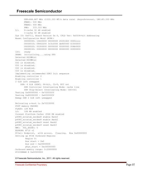
Freescale Semiconductor<br />
DDR:666.667 MHz (1333.333 MT/s data rate) (Asynchronous), LBC:83.333 MHz<br />
FMAN1: 500 MHz<br />
FMAN2: 500 MHz<br />
PME: 333.333 MHz<br />
L1: D-cache 32 kB enabled<br />
I-cache 32 kB enabled<br />
Sys ID: 0x0711, Board Version 0x 0, CPLD Ver: 0x0336-bit Addressing<br />
Reset Configuration Word (RCW):<br />
00000000: 10600000 00000000 20201820 0000cccc<br />
00000010: 08402200 3c3c2000 de800000 61000000<br />
00000020: 00300000 00000000 00000000 008b0000<br />
00000030: 00000000 00000000 00000000 00000000<br />
I2C: ready<br />
DRAM: Initializing....using SPD<br />
Detected RDIMM(s)<br />
Detected RDIMM(s)<br />
CS2 is disabled.<br />
CS3 is disabled.<br />
CS2 is disabled.<br />
CS3 is disabled.<br />
Implementing recommended DDR3 Init sequence<br />
Enabling controller 0<br />
Enabling controller 1<br />
2 GiB left unmapped<br />
DDR: 4 GiB (DDR3, 64-bit, CL=9, ECC on)<br />
DDR Controller Interleaving Mode: cache line<br />
DDR Chip-Select Interleaving Mode: CS0+CS1<br />
Testing 0x00000000 - 0x7fffffff<br />
Testing 0x80000000 - 0xffffffff<br />
Remap DDR 2 GiB left unmapped<br />
Relocating u-boot to 0x7ff30000<br />
POST memory PASSED<br />
FLASH: 128 MiB<br />
L2: 128 KB enabled<br />
Corenet Platform Cache: 2048 KB enabled<br />
p4080_erratum_serdes8 enable Bank3<br />
p4080_erratum_serdes8 enable Bank2<br />
p4080_erratum_serdes9 reset Bank2<br />
p4080_erratum_serdes9 reset Bank3<br />
MMC: FSL_ESDHC: 0<br />
EEPROM: N710 v2<br />
<strong>PCIe</strong>1: Endpoint, with errors. Clearing. Now 0x00000000<br />
Setting up PCIE Outbound Regions<br />
Region 0:<br />
bus start = 0x0<br />
bus end = 0x20000000<br />
phys_start = 0xc00000000<br />
Outbound memory range: 0:20000000<br />
PCICSRBAR @ 0xff000000<br />
© Freescale Semiconductor, Inc., 2011. All rights reserved.<br />
Freescale Confidential Proprietary Page 37


