

AN4365, Qorivva MPC56xx Flash Programming Through Nexus/JTAG
AN4365, Qorivva MPC56xx Flash Programming Through Nexus/JTAG
AN4365, Qorivva MPC56xx Flash Programming Through Nexus/JTAG

You also want an ePaper? Increase the reach of your titles
YUMPU automatically turns print PDFs into web optimized ePapers that Google loves.
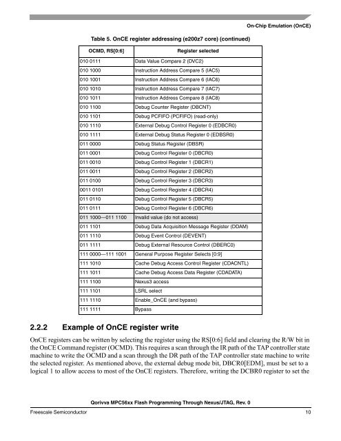
Table 5. OnCE register addressing (e200z7 core) (continued)<br />
OCMD, RS[0:6] Register selected<br />
010 0111 Data Value Compare 2 (DVC2)<br />
010 1000 Instruction Address Compare 5 (IAC5)<br />
010 1001 Instruction Address Compare 6 (IAC6)<br />
010 1010 Instruction Address Compare 7 (IAC7)<br />
010 1011 Instruction Address Compare 8 (IAC8)<br />
010 1100 Debug Counter Register (DBCNT)<br />
010 1101 Debug PCFIFO (PCFIFO) (read-only)<br />
010 1110 External Debug Control Register 0 (EDBCR0)<br />
010 1111 External Debug Status Register 0 (EDBSR0)<br />
011 0000 Debug Status Register (DBSR)<br />
011 0001 Debug Control Register 0 (DBCR0)<br />
011 0010 Debug Control Register 1 (DBCR1)<br />
011 0011 Debug Control Register 2 (DBCR2)<br />
011 0100 Debug Control Register 3 (DBCR3)<br />
0011 0101 Debug Control Register 4 (DBCR4)<br />
011 0110 Debug Control Register 5 (DBCR5)<br />
011 0111 Debug Control Register 6 (DBCR6)<br />
011 1000—011 1100 Invalid value (do not access)<br />
011 1101 Debug Data Acquisition Message Register (DDAM)<br />
011 1110 Debug Event Control (DEVENT)<br />
011 1111 Debug External Resource Control (DBERC0)<br />
111 0000—111 1001 General Purpose Register Selects [0:9]<br />
111 1010 Cache Debug Access Control Register (CDACNTL)<br />
111 1011 Cache Debug Access Data Register (CDADATA)<br />
111 1100 <strong>Nexus</strong>3 access<br />
111 1101 LSRL select<br />
111 1110 Enable_OnCE (and bypass)<br />
111 1111 Bypass<br />
2.2.2 Example of OnCE register write<br />
<strong>Qorivva</strong> <strong>MPC56xx</strong> <strong>Flash</strong> <strong>Programming</strong> <strong>Through</strong> <strong>Nexus</strong>/<strong>JTAG</strong>, Rev. 0<br />
On-Chip Emulation (OnCE)<br />
OnCE registers can be written by selecting the register using the RS[0:6] field and clearing the R/W bit in<br />
the OnCE Command register (OCMD). This requires a scan through the IR path of the TAP controller state<br />
machine to write the OCMD and a scan through the DR path of the TAP controller state machine to write<br />
the selected register. As mentioned above, the external debug mode bit, DBCR0[EDM], must be set to a<br />
logical 1 to allow access to most of the OnCE registers. Therefore, writing the DCBR0 register to set the<br />
Freescale Semiconductor 10


