

AN4365, Qorivva MPC56xx Flash Programming Through Nexus/JTAG
AN4365, Qorivva MPC56xx Flash Programming Through Nexus/JTAG
AN4365, Qorivva MPC56xx Flash Programming Through Nexus/JTAG

You also want an ePaper? Increase the reach of your titles
YUMPU automatically turns print PDFs into web optimized ePapers that Google loves.
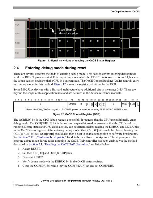
Figure 11. Signal transitions of reading the OnCE Status Register<br />
2.4 Entering debug mode during reset<br />
<strong>Qorivva</strong> <strong>MPC56xx</strong> <strong>Flash</strong> <strong>Programming</strong> <strong>Through</strong> <strong>Nexus</strong>/<strong>JTAG</strong>, Rev. 0<br />
On-Chip Emulation (OnCE)<br />
There are several different methods of entering debug mode. This section covers entering debug mode<br />
while the RESET pin is asserted. Entering debug mode while the RESET pin is asserted is useful, because<br />
the debug session begins with the CPU in a known state. The OnCE Control Register (OCR) controls entry<br />
into debug mode for this method. Figure 12 shows the register definition for the OCR.<br />
Some <strong>MPC56xx</strong> devices with a Harvard architecture have additional bits in the range 0–15. These are<br />
beyond the scope of this application note and are detailed in the device reference manuals.<br />
0 1 2 3 4 5 6 7 8 9 10 11 12 13 14 15 16 17 18 19 20 21 22 23 24 25 26 27 28 29 30 31<br />
0 DMDIS 0<br />
The OCR[DR] bit is the CPU debug request control bit; it requests that the CPU unconditionally enter<br />
debug mode. The OCR[WKUP] bit is the wakeup request bit used to guarantee that the CPU clock is<br />
running. Debug status and CPU clock activity can be determined by reading the DEBUG and MCLK bits<br />
in the OnCE status register. After entering debug mode, the OCR[DR] bit should be cleared leaving the<br />
OCR[WKUP] bit set. OCR[FDB] should also then be set to enable recognition of software breakpoints.<br />
See Section 2.12.1, “Software breakpoints,” for details on software breakpoints. The steps required for<br />
entering debug mode during reset assuming the OnCE TAP controller has been enabled via the method<br />
described in Section 2.1, “Enabling the OnCE TAP Controller,” are listed below:<br />
1. Assert RESET.<br />
2. Set the OCR[DR] and OCR[WKUP] bits.<br />
3. Deassert RESET.<br />
4. Verify debug mode via the DEBUG bit in the OnCE status register.<br />
5. Clear the OCR[DR] bit while leaving OCR[WKUP] set and set OCR[FDB].<br />
Freescale Semiconductor 14<br />
DW<br />
DI<br />
DM<br />
DG<br />
DE<br />
0 WKUP FDB<br />
Reset - 0x0000_0000 on negation of JCOMP, power on reset, or entering TEST LOGIC RESET state<br />
Figure 12. OnCE Control Register (OCR)<br />
DR


