

AN4365, Qorivva MPC56xx Flash Programming Through Nexus/JTAG
AN4365, Qorivva MPC56xx Flash Programming Through Nexus/JTAG
AN4365, Qorivva MPC56xx Flash Programming Through Nexus/JTAG

Create successful ePaper yourself
Turn your PDF publications into a flip-book with our unique Google optimized e-Paper software.
2.6.1 Instruction Register (IR)<br />
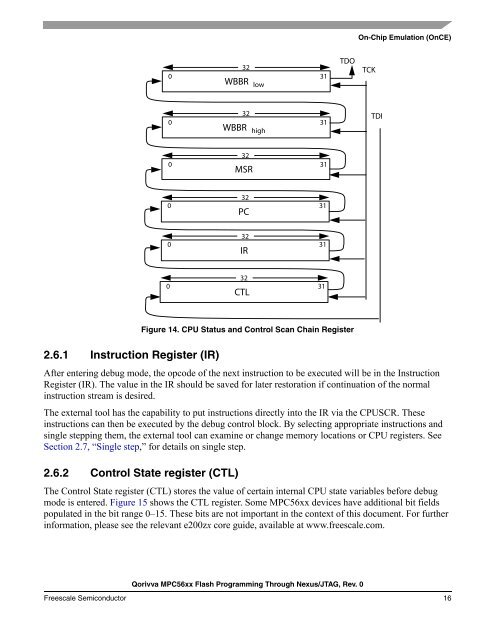
Figure 14. CPU Status and Control Scan Chain Register<br />
<strong>Qorivva</strong> <strong>MPC56xx</strong> <strong>Flash</strong> <strong>Programming</strong> <strong>Through</strong> <strong>Nexus</strong>/<strong>JTAG</strong>, Rev. 0<br />
On-Chip Emulation (OnCE)<br />
After entering debug mode, the opcode of the next instruction to be executed will be in the Instruction<br />
Register (IR). The value in the IR should be saved for later restoration if continuation of the normal<br />
instruction stream is desired.<br />
The external tool has the capability to put instructions directly into the IR via the CPUSCR. These<br />
instructions can then be executed by the debug control block. By selecting appropriate instructions and<br />
single stepping them, the external tool can examine or change memory locations or CPU registers. See<br />
Section 2.7, “Single step,” for details on single step.<br />
2.6.2 Control State register (CTL)<br />
0<br />
32<br />
WBBR low<br />
31<br />
0<br />
32<br />
WBBR high<br />
31<br />
32<br />
0 31<br />
MSR<br />
32<br />
0 31<br />
PC<br />
32<br />
0 31<br />
IR<br />
32<br />
0 31<br />
CTL<br />
The Control State register (CTL) stores the value of certain internal CPU state variables before debug<br />
mode is entered. Figure 15 shows the CTL register. Some <strong>MPC56xx</strong> devices have additional bit fields<br />
populated in the bit range 0–15. These bits are not important in the context of this document. For further<br />
information, please see the relevant e200zx core guide, available at www.freescale.com.<br />
Freescale Semiconductor 16<br />
TDO<br />
TCK<br />
TDI


