

AN4365, Qorivva MPC56xx Flash Programming Through Nexus/JTAG
AN4365, Qorivva MPC56xx Flash Programming Through Nexus/JTAG
AN4365, Qorivva MPC56xx Flash Programming Through Nexus/JTAG

Create successful ePaper yourself
Turn your PDF publications into a flip-book with our unique Google optimized e-Paper software.
5.2 Tool requirements<br />
<strong>Qorivva</strong> <strong>MPC56xx</strong> <strong>Flash</strong> <strong>Programming</strong> <strong>Through</strong> <strong>Nexus</strong>/<strong>JTAG</strong>, Rev. 0<br />
Creating the flash programming tool<br />
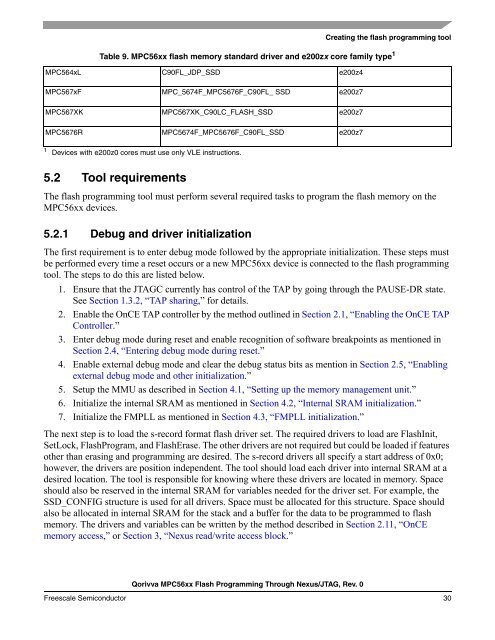
Table 9. <strong>MPC56xx</strong> flash memory standard driver and e200zx core family type 1<br />
MPC564xL C90FL_JDP_SSD e200z4<br />
MPC567xF MPC_5674F_MPC5676F_C90FL_ SSD e200z7<br />
MPC567XK MPC567XK_C90LC_FLASH_SSD e200z7<br />
MPC5676R MPC5674F_MPC5676F_C90FL_SSD e200z7<br />
1 Devices with e200z0 cores must use only VLE instructions.<br />
The flash programming tool must perform several required tasks to program the flash memory on the<br />
<strong>MPC56xx</strong> devices.<br />
5.2.1 Debug and driver initialization<br />
The first requirement is to enter debug mode followed by the appropriate initialization. These steps must<br />
be performed every time a reset occurs or a new <strong>MPC56xx</strong> device is connected to the flash programming<br />
tool. The steps to do this are listed below.<br />
1. Ensure that the <strong>JTAG</strong>C currently has control of the TAP by going through the PAUSE-DR state.<br />
See Section 1.3.2, “TAP sharing,” for details.<br />
2. Enable the OnCE TAP controller by the method outlined in Section 2.1, “Enabling the OnCE TAP<br />
Controller.”<br />
3. Enter debug mode during reset and enable recognition of software breakpoints as mentioned in<br />
Section 2.4, “Entering debug mode during reset.”<br />
4. Enable external debug mode and clear the debug status bits as mention in Section 2.5, “Enabling<br />
external debug mode and other initialization.”<br />
5. Setup the MMU as described in Section 4.1, “Setting up the memory management unit.”<br />
6. Initialize the internal SRAM as mentioned in Section 4.2, “Internal SRAM initialization.”<br />
7. Initialize the FMPLL as mentioned in Section 4.3, “FMPLL initialization.”<br />
The next step is to load the s-record format flash driver set. The required drivers to load are <strong>Flash</strong>Init,<br />
SetLock, <strong>Flash</strong>Program, and <strong>Flash</strong>Erase. The other drivers are not required but could be loaded if features<br />
other than erasing and programming are desired. The s-record drivers all specify a start address of 0x0;<br />
however, the drivers are position independent. The tool should load each driver into internal SRAM at a<br />
desired location. The tool is responsible for knowing where these drivers are located in memory. Space<br />
should also be reserved in the internal SRAM for variables needed for the driver set. For example, the<br />
SSD_CONFIG structure is used for all drivers. Space must be allocated for this structure. Space should<br />
also be allocated in internal SRAM for the stack and a buffer for the data to be programmed to flash<br />
memory. The drivers and variables can be written by the method described in Section 2.11, “OnCE<br />
memory access,” or Section 3, “<strong>Nexus</strong> read/write access block.”<br />
Freescale Semiconductor 30


