AN4365, Qorivva MPC56xx Flash Programming Through Nexus/JTAG
AN4365, Qorivva MPC56xx Flash Programming Through Nexus/JTAG
AN4365, Qorivva MPC56xx Flash Programming Through Nexus/JTAG
Create successful ePaper yourself
Turn your PDF publications into a flip-book with our unique Google optimized e-Paper software.
<strong>Qorivva</strong> <strong>MPC56xx</strong> <strong>Flash</strong> <strong>Programming</strong> <strong>Through</strong> <strong>Nexus</strong>/<strong>JTAG</strong>, Rev. 0<br />
<strong>Nexus</strong> read/write access block<br />
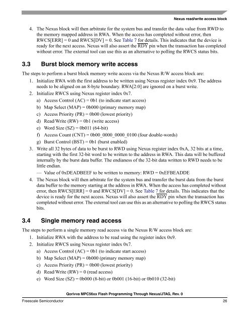
4. The <strong>Nexus</strong> block will then arbitrate for the system bus and transfer the data value from RWD to<br />
the memory mapped address in RWA. When the access has completed without error, then<br />
RWCS[ERR] = 0 and RWCS[DV] = 0. See Table 7 for details. This indicates that the device is<br />
ready for the next access. <strong>Nexus</strong> will also assert the RDY pin when the transaction has completed<br />
without error. The external tool can use this as an alternative to polling the RWCS status bits.<br />
3.3 Burst block memory write access<br />
The steps to perform a burst block memory write access via the <strong>Nexus</strong> R/W access block are:<br />
1. Initialize RWA with the first address to be written using <strong>Nexus</strong> register index 0x9. The address<br />
needs to be aligned on an 8-byte boundary. RWA[2:0] are ignored on a burst write.<br />
2. Initialize RWCS using <strong>Nexus</strong> register index 0x7.<br />
a) Access Control (AC) = 0b1 (to indicate start access)<br />
b) Map Select (MAP) = 0b000 (primary memory map)<br />
c) Access Priority (PR) = 0b00 (lowest priority)<br />
d) Read/Write (RW) = 0b1 (write access)<br />
e) Word Size (SZ) = 0b011 (64-bit)<br />
f) Access Count (CNT) = 0b00_0000_0000_0100 (four double-words)<br />
g) Burst Control (BST) = 0b1 (burst enabled)<br />
3. Write all 32 bytes of data to be burst to RWD using <strong>Nexus</strong> register index 0xA, 32 bits at a time,<br />
starting with the first 32-bit word to be written to the address in RWA. This data will be buffered<br />
internally by the burst data buffer. The endianess of the 32-bit data written to RWD needs to be<br />
little endian.<br />
— Value of 0xDEADBEEF to be written to memory: RWD = 0xEFBEADDE<br />
4. The <strong>Nexus</strong> block will then arbitrate for the system bus and transfer the burst data from the burst<br />
data buffer to the memory starting at the address in RWA. When the access has completed without<br />
error, then RWCS[ERR] = 0 and RWCS[DV] = 0. See Table 7 for details. This indicates that the<br />
device is ready for the next access. <strong>Nexus</strong> will also assert the RDY pin when the transaction has<br />
completed without error. The external tool can use this as an alternative to polling the RWCS status<br />
bits.<br />
3.4 Single memory read access<br />
The steps to perform a single memory read access via the <strong>Nexus</strong> R/W access block are:<br />
1. Initialize RWA with the address to be read using the register index 0x9.<br />
2. Initialize RWCS using <strong>Nexus</strong> register index 0x7.<br />
a) Access Control (AC) = 0b1 (to indicate start access)<br />
b) Map Select (MAP) = 0b000 (primary memory map)<br />
c) Access Priority (PR) = 0b00 (lowest priority)<br />
d) Read/Write (RW) = 0 (read access)<br />
e) Word Size (SZ) = 0b000 (8-bit) or 0b001 (16-bit) or 0b010 (32-bit)<br />
Freescale Semiconductor 26


