

AN4365, Qorivva MPC56xx Flash Programming Through Nexus/JTAG
AN4365, Qorivva MPC56xx Flash Programming Through Nexus/JTAG
AN4365, Qorivva MPC56xx Flash Programming Through Nexus/JTAG

Create successful ePaper yourself
Turn your PDF publications into a flip-book with our unique Google optimized e-Paper software.
4.1 Setting up the memory management unit<br />
<strong>Qorivva</strong> <strong>MPC56xx</strong> <strong>Flash</strong> <strong>Programming</strong> <strong>Through</strong> <strong>Nexus</strong>/<strong>JTAG</strong>, Rev. 0<br />
System initialization<br />
<strong>MPC56xx</strong> devices with an e200z0 core do not have a memory management unit (MMU). The memory<br />
locations are permanently mapped and setting up the MMU is not required.<br />
The MMU on the non-e200z0 <strong>MPC56xx</strong> devices provides access protection to memory mapped regions<br />
as well as memory translation from effective to real addresses. For the purpose of flash memory<br />
programming, it is easiest to setup the MMU such that the effective addresses are the same as the real<br />
addresses. For the CPU to access a memory mapped region, an MMU entry for that memory space must<br />
be configured. The external tool has the capability to setup MMU entries by writing the appropriate SPRs<br />
and single stepping over the tlbwe instruction.<br />
For flash memory programming, the external tool should set up at least four MMU entries. The steps<br />
required to setup an MMU entry are:<br />
1. Set up MAS0 (SPR 624).<br />
2. Set up MAS1 (SPR 625).<br />
3. Set up MAS2 (SPR 626).<br />
4. Set up MAS3 (SPR 627).<br />
5. Execute tlbwe (0x7C0007A4).<br />
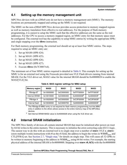
The minimum set of four MMU entries required is detailed in Table 8. This example for setting up the<br />
MMU is for an external tool using the Freescale provided non-VLE <strong>Flash</strong> drivers running from internal<br />
SRAM. For the VLE driver set, MAS2 value for the internal SRAM should be 0x40000028 to enable the<br />
MAS2[VLE] bit.<br />
4.2 Internal SRAM initialization<br />
Table 8. MAS register settings for MMU setup<br />
Memory region MAS0 MAS1 MAS2 MAS3<br />
PBridge B 1<br />
0x10000000 0xC0000500 0xFFF0000A 0xFFF0003F<br />
Internal SRAM 0x10010000 0xC0000400 0x400000082 0x4000003F<br />
PBridge A 0x10020000 0xC0000500 0xC3F00008 0xC3F0003F<br />
Internal flash 0x10030000 0xC0000700 0x00000000 0x0000003F<br />
1 The PBridge B MMU entry is not required for flash memory programming, but this MMU<br />
entry in addition to the others allows access to the entire memory map of the <strong>MPC56xx</strong><br />
devices.<br />
2<br />
Set Internal SRAM MAS2 value to 0x40000028 when using the VLE driver set.<br />
The <strong>MPC56xx</strong> family of devices all contain internal SRAM that must be initialized after power-on reset<br />
by 64-bit writes to the entire memory. This is necessary to initialize the error-correcting code (ECC) logic.<br />
The easiest way to do this with an external tool is to single step over a number of stmw (VLE e_stmw)<br />
(store multiple words) instructions with r0 as the rS field, the address to begin the writes in WBBR low , and<br />
CTL[FFRA] set. See Section 2.7, “Single step,” for details on single step. This will cause all 32 GPRs to<br />
be written to memory beginning at the address in WBBR low using 64-bit writes. For example, the starting<br />
physical address of the internal SRAM is 0x40000000. Stepping over stmw r0, 0(X) with the 0x40000000<br />
Freescale Semiconductor 28


