

AN4365, Qorivva MPC56xx Flash Programming Through Nexus/JTAG
AN4365, Qorivva MPC56xx Flash Programming Through Nexus/JTAG
AN4365, Qorivva MPC56xx Flash Programming Through Nexus/JTAG

Create successful ePaper yourself
Turn your PDF publications into a flip-book with our unique Google optimized e-Paper software.
<strong>Qorivva</strong> <strong>MPC56xx</strong> <strong>Flash</strong> <strong>Programming</strong> <strong>Through</strong> <strong>Nexus</strong>/<strong>JTAG</strong>, Rev. 0<br />
<strong>Nexus</strong> read/write access block<br />
4. Poll the DBSR for the appropriate status bit to be set; DBSR[IAC1], DBSR[IAC2], DBSR[IAC3],<br />
or DBSR[IAC4]. Figure 13 shows the register definition of DBSR.<br />
5. If the appropriate status bit in DBSR is set, verify entry into debug mode by reading the OnCE<br />
status register.<br />
6. Clear the appropriate status bit by writing a 1 to that bit location in the DBSR; DBSR[IAC1],<br />
DBSR[IAC2], DBSR[IAC3], or DBSR[IAC4].<br />
3 <strong>Nexus</strong> read/write access block<br />
The <strong>Nexus</strong> module provided on the cores of the <strong>MPC56xx</strong> family of devices offers the capability for<br />
program trace, data trace, ownership trace, watchpoint messaging and trigger, and read/write (R/W) access<br />
to memory mapped regions. This section covers R/W access using the <strong>Nexus</strong> R/W access block. The other<br />
features of the <strong>Nexus</strong> module are beyond the scope of this document and will not be covered. Some<br />
versions of the <strong>MPC56xx</strong> devices with an e200z0 core do not have a <strong>Nexus</strong> read/write access block.<br />
Further details can be found in AN4088, “MPC5500/MPC5600 <strong>Nexus</strong> Support Overview.”<br />
Unlike the OnCE method of memory access, the <strong>Nexus</strong> R/W access block provides the ability to read and<br />
write memory without having to stop code execution by entering debug mode. The <strong>Nexus</strong> R/W access<br />
method provides faster memory access over the OnCE method due to fewer <strong>JTAG</strong> scans, and it doesn’t<br />
require loading and single stepping over any instructions. The <strong>Nexus</strong> R/W access block is independent of<br />
the CPU and therefore bypasses the MMU and cache.<br />
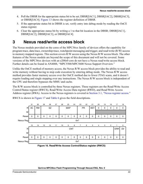
The R/W access block is controlled by three <strong>Nexus</strong> registers. These registers are the Read/Write Access<br />
Control/Status register (RWCS), Read/Write Access Data register (RWD), and Read/Write Access<br />
Address register (RWA). Access to the <strong>Nexus</strong> registers is covered in Section 3.1, “<strong>Nexus</strong> register access.”<br />
RWCS is shown in Figure 17 and Table 6 gives the field descriptions.<br />
31 30 29 28 27 26 25 24 23 22 21 20 19 18 17 16<br />
R AC RW SZ MAP PR BST 0 0 0 0 0<br />
W<br />
Reset 0 0 0 0 0 0 0 0 0 0 0 0 0 0 0 0<br />
<strong>Nexus</strong> Reg 0x7<br />
15 14 13 12 11 10 9 8 7 6 5 4 3 2 1 0<br />
R CNT ERR DV<br />
W<br />
Reset 0 0 0 0 0 0 0 0 0 0 0 0 0 0 0 0<br />
<strong>Nexus</strong> Reg 0x7<br />
Figure 16. Read/Write Access Control/Status register (RWCS)<br />
Freescale Semiconductor 22


