24-Bit, 192-kHz Sampling, Advanced Segment, Audio Stereo DAC ...
24-Bit, 192-kHz Sampling, Advanced Segment, Audio Stereo DAC ...
24-Bit, 192-kHz Sampling, Advanced Segment, Audio Stereo DAC ...

Create successful ePaper yourself
Turn your PDF publications into a flip-book with our unique Google optimized e-Paper software.
www.ti.com<br />
AUDIO DATA INTERFACE<br />
<strong>Audio</strong> Serial Interface<br />
<br />
SLES105B − FEBRUARY 2004 − REVISED NOVEMBER 2006<br />
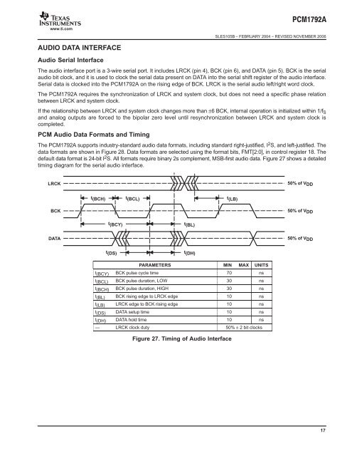
The audio interface port is a 3-wire serial port. It includes LRCK (pin 4), BCK (pin 6), and DATA (pin 5). BCK is the serial<br />
audio bit clock, and it is used to clock the serial data present on DATA into the serial shift register of the audio interface.<br />
Serial data is clocked into the PCM1792A on the rising edge of BCK. LRCK is the serial audio left/right word clock.<br />
The PCM1792A requires the synchronization of LRCK and system clock, but does not need a specific phase relation<br />
between LRCK and system clock.<br />
If the relationship between LRCK and system clock changes more than ±6 BCK, internal operation is initialized within 1/fS<br />
and analog outputs are forced to the bipolar zero level until resynchronization between LRCK and system clock is<br />
completed.<br />
PCM <strong>Audio</strong> Data Formats and Timing<br />
The PCM1792A supports industry-standard audio data formats, including standard right-justified, I 2 S, and left-justified. The<br />
data formats are shown in Figure 28. Data formats are selected using the format bits, FMT[2:0], in control register 18. The<br />
default data format is <strong>24</strong>-bit I 2 S. All formats require binary 2s complement, MSB-first audio data. Figure 27 shows a detailed<br />
timing diagram for the serial audio interface.<br />
LRCK<br />
BCK<br />
DATA<br />
t(BCH)<br />
t(BCY)<br />
t(DS)<br />
t(BCL)<br />
t(BL)<br />
t(DH)<br />
t(LB)<br />
PARAMETERS MIN MAX UNITS<br />
t(BCY) BCK pulse cycle time 70 ns<br />
t(BCL) BCK pulse duration, LOW 30 ns<br />
t(BCH) BCK pulse duration, HIGH 30 ns<br />
t(BL) BCK rising edge to LRCK edge 10 ns<br />
t(LB) LRCK edge to BCK rising edge 10 ns<br />
t(DS) DATA setup time 10 ns<br />
t(DH) DATA hold time 10 ns<br />
— LRCK clock duty 50% ± 2 bit clocks<br />
Figure 27. Timing of <strong>Audio</strong> Interface<br />
50% of VDD<br />
50% of VDD<br />
50% of VDD<br />
17