24-Bit, 192-kHz Sampling, Advanced Segment, Audio Stereo DAC ...
24-Bit, 192-kHz Sampling, Advanced Segment, Audio Stereo DAC ...
24-Bit, 192-kHz Sampling, Advanced Segment, Audio Stereo DAC ...

Create successful ePaper yourself
Turn your PDF publications into a flip-book with our unique Google optimized e-Paper software.
www.ti.com<br />
SYSTEM CLOCK AND RESET FUNCTIONS<br />
System Clock Input<br />
<br />
SLES105B − FEBRUARY 2004 − REVISED NOVEMBER 2006<br />
The PCM1792A requires a system clock for operating the digital interpolation filters and advanced segment <strong>DAC</strong><br />
modulators. The system clock is applied at the SCK input (pin 7). The PCM1792A has a system clock detection circuit that<br />
automatically senses if the system clock is operating between 128 fS and 768 fS. Table 1 shows examples of system clock<br />
frequencies for common audio sampling rates. If the oversampling rate of the delta-sigma modulator is selected as 128 fS,<br />
the system clock frequency is over 256 fS.<br />
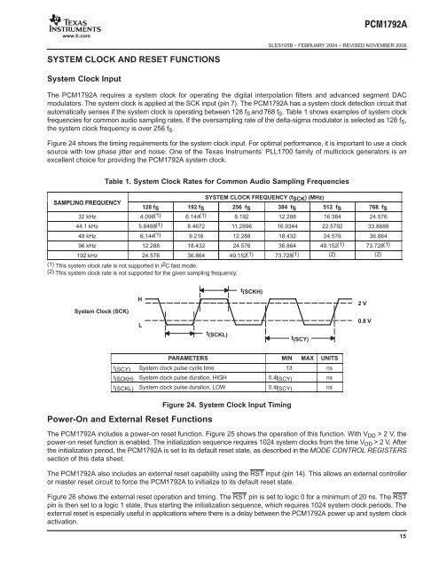
Figure <strong>24</strong> shows the timing requirements for the system clock input. For optimal performance, it is important to use a clock<br />
source with low phase jitter and noise. One of the Texas Instruments’ PLL1700 family of multiclock generators is an<br />
excellent choice for providing the PCM1792A system clock.<br />
Table 1. System Clock Rates for Common <strong>Audio</strong> <strong>Sampling</strong> Frequencies<br />
SAMPLING FREQUENCY<br />
128 fS<br />
SYSTEM CLOCK FREQUENCY (fSCK) (MHz)<br />
<strong>192</strong> fS 256 fS 384 fS 512 fS 768 fS<br />
32 <strong>kHz</strong> 4.096(1) 6.144(1) 8.<strong>192</strong> 12.288 16.384 <strong>24</strong>.576<br />
44.1 <strong>kHz</strong> 5.6488(1) 8.4672 11.2896 16.9344 22.5792 33.8688<br />
48 <strong>kHz</strong> 6.144(1) 9.216 12.288 18.432 <strong>24</strong>.576 36.864<br />
96 <strong>kHz</strong> 12.288 18.432 <strong>24</strong>.576 36.864 49.152(1) 73.728(1)<br />
<strong>192</strong> <strong>kHz</strong> <strong>24</strong>.576 36.864 49.152(1) 73.728(1) (2) (2)<br />
(1) This system clock rate is not supported in I2C fast mode.<br />
(2) This system clock rate is not supported for the given sampling frequency.<br />
System Clock (SCK)<br />
H<br />
L<br />
t(SCKL)<br />
t(SCKH)<br />
t(SCY)<br />
PARAMETERS MIN MAX UNITS<br />
t(SCY) System clock pulse cycle time 13 ns<br />
t(SCKH) System clock pulse duration, HIGH 0.4 t(SCY) ns<br />
t(SCKL) System clock pulse duration, LOW 0.4 t(SCY) ns<br />
Power-On and External Reset Functions<br />
Figure <strong>24</strong>. System Clock Input Timing<br />
The PCM1792A includes a power-on reset function. Figure 25 shows the operation of this function. With VDD > 2 V, the<br />
power-on reset function is enabled. The initialization sequence requires 10<strong>24</strong> system clocks from the time VDD > 2 V. After<br />
the initialization period, the PCM1792A is set to its default reset state, as described in the MODE CONTROL REGISTERS<br />
section of this data sheet.<br />
The PCM1792A also includes an external reset capability using the RST input (pin 14). This allows an external controller<br />
or master reset circuit to force the PCM1792A to initialize to its default reset state.<br />
Figure 26 shows the external reset operation and timing. The RST pin is set to logic 0 for a minimum of 20 ns. The RST<br />
pin is then set to a logic 1 state, thus starting the initialization sequence, which requires 10<strong>24</strong> system clock periods. The<br />
external reset is especially useful in applications where there is a delay between the PCM1792A power up and system clock<br />
activation.<br />
2 V<br />
0.8 V<br />
15