24-Bit, 192-kHz Sampling, Advanced Segment, Audio Stereo DAC ...
24-Bit, 192-kHz Sampling, Advanced Segment, Audio Stereo DAC ...
24-Bit, 192-kHz Sampling, Advanced Segment, Audio Stereo DAC ...

You also want an ePaper? Increase the reach of your titles
YUMPU automatically turns print PDFs into web optimized ePapers that Google loves.
www.ti.com<br />
Write Register<br />
<br />
SLES105B − FEBRUARY 2004 − REVISED NOVEMBER 2006<br />
A master can write to any PCM1792A registers using single or multiple accesses. The master sends a PCM1792A slave<br />
address with a write bit, a register address, and the data. If multiple access is required, the address is that of the starting<br />
register, followed by the data to be transferred. When the data are received properly, the index register is incremented by<br />
1 automatically. When the index register reaches 0x7F, the next value is 0x0. When undefined registers are accessed, the<br />
PCM1792A does not send an acknowledgement. Figure 33 is a diagram of the write operation.<br />
Transmitter M M M S M S M<br />
Data Type St Slave Address W ACK Reg Address ACK Write Data 1<br />
Read Register<br />
M: Master Device S: Slave Device<br />
St: Start Condition ACK: Acknowledge Sp: Stop Condition W: Write<br />
Figure 33. Write Operation<br />
S<br />
ACK<br />
M<br />
Write Data 2<br />
A master can read the PCM1792A register. The value of the register address is stored in an indirect index register in<br />
advance. The master sends a PCM1792A slave address with a read bit after storing the register address. Then the<br />
PCM1792A transfers the data which the index register points to. When the data are transferred during a multiple access,<br />
the index register is incremented by 1 automatically. (When first going into read mode immediately following a write, the<br />
index register is not incremented. The master can read the register that was previously written.) When the index register<br />
reaches 0x7F, the next value is 0x0. The PCM1792A outputs some data when the index register is 0x10 to 0x1F, even if<br />
it is not defined in Table 4. Figure 34 is a diagram of the read operation.<br />
Transmitter M M M S M S M M<br />
Data Type St Slave Address W ACK Reg Address ACK Sr Slave Address<br />
S<br />
ACK<br />
Data<br />
S<br />
ACK<br />
Slave M<br />
M: Master Device S: Slave Device<br />
St: Start Condition Sr: Repeated Start Condition ACK: Acknowledge Sp: Stop Condition NACK: Not Acknowledge<br />
W: Write R: Read<br />
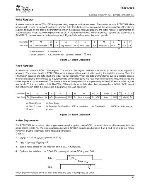
Noise Suppression<br />
Figure 34. Read Operation<br />
The PCM1792A incorporates noise suppression using the system clock (SCK). However, there must be no more than two<br />
noise spikes in 600 ns. The noise suppression works for SCK frequencies between 8 MHz and 40 MHz in fast mode.<br />
However, it works incorrectly in the following conditions.<br />
Case 1:<br />
1. t (SCK) > 120 ns (t (SCK): period of SCK)<br />
2. t (HI) + t (D−HD) < t (SCK) × 5<br />
3. Spike noise exists on the first half of the SCL HIGH pulse.<br />
4. Spike noise exists on the SDA HIGH pulse just before SDA goes LOW.<br />
SCL<br />
SDA<br />
Noise<br />
When these conditions occur at the same time, the data is recognized as LOW.<br />
M<br />
R<br />
ACK<br />
S<br />
ACK<br />
S<br />
NACK<br />
M<br />
Sp<br />
M<br />
Sp<br />
23