The Future of Instrumentation - High Frequency Electronics
The Future of Instrumentation - High Frequency Electronics
The Future of Instrumentation - High Frequency Electronics

Create successful ePaper yourself
Turn your PDF publications into a flip-book with our unique Google optimized e-Paper software.
<strong>High</strong> <strong>Frequency</strong> Design<br />
EM Simulator<br />
(Continued from page 38)<br />
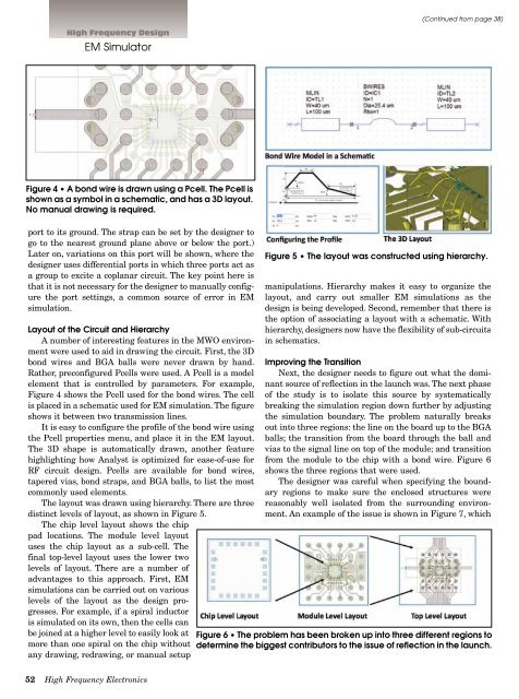
Figure 4 • A bond wire is drawn using a Pcell. <strong>The</strong> Pcell is<br />
shown as a symbol in a schematic, and has a 3D layout.<br />
No manual drawing is required.<br />
port to its ground. <strong>The</strong> strap can be set by the designer to<br />
go to the nearest ground plane above or below the port.)<br />
Later on, variations on this port will be shown, where the<br />
designer uses differential ports in which three ports act as<br />
a group to excite a coplanar circuit. <strong>The</strong> key point here is<br />
that it is not necessary for the designer to manually configure<br />
the port settings, a common source <strong>of</strong> error in EM<br />
simulation.<br />
Layout <strong>of</strong> the Circuit and Hierarchy<br />
A number <strong>of</strong> interesting features in the MWO environment<br />
were used to aid in drawing the circuit. First, the 3D<br />
bond wires and BGA balls were never drawn by hand.<br />
Rather, preconfigured Pcells were used. A Pcell is a model<br />
element that is controlled by parameters. For example,<br />
Figure 4 shows the Pcell used for the bond wires. <strong>The</strong> cell<br />
is placed in a schematic used for EM simulation. <strong>The</strong> figure<br />
shows it between two transmission lines.<br />
It is easy to configure the pr<strong>of</strong>ile <strong>of</strong> the bond wire using<br />
the Pcell properties menu, and place it in the EM layout.<br />
<strong>The</strong> 3D shape is automatically drawn, another feature<br />
highlighting how Analyst is optimized for ease-<strong>of</strong>-use for<br />
RF circuit design. Pcells are available for bond wires,<br />
tapered vias, bond straps, and BGA balls, to list the most<br />
commonly used elements.<br />
<strong>The</strong> layout was drawn using hierarchy. <strong>The</strong>re are three<br />
distinct levels <strong>of</strong> layout, as shown in Figure 5.<br />
<strong>The</strong> chip level layout shows the chip<br />
pad locations. <strong>The</strong> module level layout<br />
uses the chip layout as a sub-cell. <strong>The</strong><br />
final top-level layout uses the lower two<br />
levels <strong>of</strong> layout. <strong>The</strong>re are a number <strong>of</strong><br />
advantages to this approach. First, EM<br />
simulations can be carried out on various<br />
levels <strong>of</strong> the layout as the design progresses.<br />
For example, if a spiral inductor<br />
is simulated on its own, then the cells can<br />
be joined at a higher level to easily look at<br />
more than one spiral on the chip without<br />
any drawing, redrawing, or manual setup<br />
Figure 5 • <strong>The</strong> layout was constructed using hierarchy.<br />
manipulations. Hierarchy makes it easy to organize the<br />
layout, and carry out smaller EM simulations as the<br />
design is being developed. Second, remember that there is<br />
the option <strong>of</strong> associating a layout with a schematic. With<br />
hierarchy, designers now have the flexibility <strong>of</strong> sub-circuits<br />
in schematics.<br />
Improving the Transition<br />
Next, the designer needs to figure out what the dominant<br />
source <strong>of</strong> reflection in the launch was. <strong>The</strong> next phase<br />
<strong>of</strong> the study is to isolate this source by systematically<br />
breaking the simulation region down further by adjusting<br />
the simulation boundary. <strong>The</strong> problem naturally breaks<br />
out into three regions: the line on the board up to the BGA<br />
balls; the transition from the board through the ball and<br />
vias to the signal line on top <strong>of</strong> the module; and transition<br />
from the module to the chip with a bond wire. Figure 6<br />
shows the three regions that were used.<br />
<strong>The</strong> designer was careful when specifying the boundary<br />
regions to make sure the enclosed structures were<br />
reasonably well isolated from the surrounding environment.<br />
An example <strong>of</strong> the issue is shown in Figure 7, which<br />
Figure 6 • <strong>The</strong> problem has been broken up into three different regions to<br />
determine the biggest contributors to the issue <strong>of</strong> reflection in the launch.<br />
52 <strong>High</strong> <strong>Frequency</strong> <strong>Electronics</strong>