The Future of Instrumentation - High Frequency Electronics
The Future of Instrumentation - High Frequency Electronics
The Future of Instrumentation - High Frequency Electronics

You also want an ePaper? Increase the reach of your titles
YUMPU automatically turns print PDFs into web optimized ePapers that Google loves.
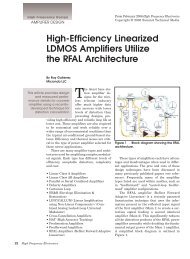
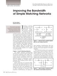
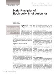
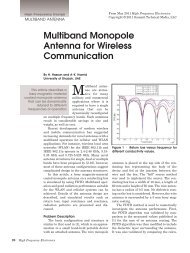
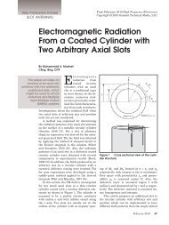
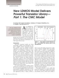
<strong>High</strong> <strong>Frequency</strong> Design<br />
EM Simulator<br />
Figure 9 • <strong>The</strong> bond wire region is modified<br />
by doubling the bond wires, and reducing<br />
the gap from the pad to the side<br />
grounds. <strong>The</strong> ground vias on the board<br />
are moved away from the ground balls<br />
for increased inductance.<br />
To physically realize the extra capacitance near the<br />
bond wire, a variety <strong>of</strong> techniques were tried, including<br />
doubling the bond wires to reduce their inductance and<br />
narrowing the gaps between the line and the side grounds<br />
in the module. <strong>The</strong> extra inductance near the BGA balls<br />
was accomplished by adding extra loop length to the<br />
ground return on the board. <strong>The</strong> final solution is shown in<br />
Figure 9.<br />
<strong>The</strong> ground vias on the board were moved away from<br />
the ground balls for increased inductance. <strong>The</strong> top diagram<br />
in the figure shows the bond wire has been doubled and<br />
shortened to reduce inductance. <strong>The</strong> gap between the bond<br />
wire pad and side grounds has been decreased to increase<br />
capacitance. <strong>The</strong> bottom figure shows the ground vias on<br />
the board being moved away from the ground balls to<br />
increase the loop inductance to compensate for the ball<br />
capacitance. <strong>The</strong> line on the module near the ball was also<br />
narrowed to increase inductance.<br />
Finally, the entire structure was simulated for verification,<br />
as shown in Figure 10. <strong>The</strong> mesh is not shown in the<br />
air region for visual clarity. <strong>The</strong> return loss meets the<br />
desired specification, being less than -20dB over the frequency<br />
range <strong>of</strong> interest.<br />
56 <strong>High</strong> <strong>Frequency</strong> <strong>Electronics</strong><br />
Conclusion<br />
Within this design example,<br />
AWR’s Analyst finite<br />
element 3D EM simulator<br />
was used to optimize the<br />
return loss for a board-tomodule-to-chip<br />
transition.<br />
<strong>The</strong> novel features <strong>of</strong> Analyst<br />
were leveraged to speed up<br />
the study. Portions <strong>of</strong> the<br />
layout were simulated by<br />
redefining the simulation<br />
boundary and ports, without<br />
ever needing to manually<br />
redraw the structure. Pcells<br />
for the layout <strong>of</strong> the bond<br />
wires and BGA balls were<br />
used, so that these structures<br />
did not need to be<br />
manually drawn either. By<br />
adding extra internal ports,<br />
capacitance could be added<br />
to the parts <strong>of</strong> the transition<br />
quickly, and then the values<br />
could be tuned and optimized<br />
to determine where<br />
changes were needed. <strong>The</strong><br />
preconfigured circuit simulation<br />
features in Analyst<br />
significantly reduced development<br />
time in this example:<br />
ports were automatically<br />
configured for optimal settings, 3D shapes were already<br />
drawn with Pcells, hierarchy <strong>of</strong> layout could be used, and<br />
simulation regions could easily be changed.<br />
Figure 10 • <strong>The</strong> whole layout is simulated.<br />
<strong>The</strong> return loss meets the specification <strong>of</strong><br />
being less than -20 dB over the desired<br />
frequency range.<br />
About the Author:<br />
John Dunn is AWR Corp.’s electromagnetic technologist<br />
and is also in charge <strong>of</strong> training and university program<br />
development. His area <strong>of</strong> expertise is electromagnetic<br />
theory, simulation, and modeling. Dr. Dunn’s past<br />
experience includes both the worlds <strong>of</strong> industry and academia.<br />
Prior to joining AWR, he served for four years as<br />
head <strong>of</strong> the interconnect modeling group at Tektronix,<br />
Beaverton, OR. Before entering the engineering industry,<br />
Dr. Dunn was a pr<strong>of</strong>essor <strong>of</strong> electrical engineering at the<br />
University <strong>of</strong> Colorado, Boulder from 1986 to 2001, where<br />
he lead a research group in the areas <strong>of</strong> electromagnetic<br />
simulation and modeling. Dr. Dunn received his Ph.D. and<br />
M.S. degrees in applied physics from Harvard University,<br />
Cambridge, MA, and his B.A. in physics from Carleton<br />
College, Northfield, MN. He is a senior member <strong>of</strong> IEEE<br />
and has authored papers and presented at numerous conferences<br />
and symposia throughout the world.<br />
Note: Analyst TM is a trademark <strong>of</strong> AWR Corp.