

Implementing Audio IP in SDI II on Arria V Development Board - Altera
Implementing Audio IP in SDI II on Arria V Development Board - Altera
Implementing Audio IP in SDI II on Arria V Development Board - Altera

Create successful ePaper yourself
Turn your PDF publications into a flip-book with our unique Google optimized e-Paper software.
8<br />
Runn<str<strong>on</strong>g>in</str<strong>on</strong>g>g the Reference Design<br />
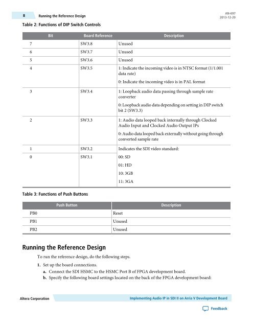
Table 2: Functi<strong>on</strong>s of D<str<strong>on</strong>g>IP</str<strong>on</strong>g> Switch C<strong>on</strong>trols<br />
AN-697<br />
2013-12-20<br />
7<br />
6<br />
5<br />
4<br />
3<br />
2<br />
1<br />
0<br />
Bit<br />
<strong>Board</strong> Reference<br />
SW3.8<br />
SW3.7<br />
SW3.6<br />
SW3.5<br />
SW3.4<br />
SW3.3<br />
SW3.2<br />
SW3.1<br />
Unused<br />
Unused<br />
Unused<br />
Descripti<strong>on</strong><br />
1: Indicate the <str<strong>on</strong>g>in</str<strong>on</strong>g>com<str<strong>on</strong>g>in</str<strong>on</strong>g>g video is <str<strong>on</strong>g>in</str<strong>on</strong>g> NTSC format (1/1.001<br />
data rate)<br />
0: Indicate the <str<strong>on</strong>g>in</str<strong>on</strong>g>com<str<strong>on</strong>g>in</str<strong>on</strong>g>g video is <str<strong>on</strong>g>in</str<strong>on</strong>g> PAL format<br />
1: Loopback audio data pass<str<strong>on</strong>g>in</str<strong>on</strong>g>g through sample rate<br />
c<strong>on</strong>verter<br />
0: Loopback audio data depend<str<strong>on</strong>g>in</str<strong>on</strong>g>g <strong>on</strong> sett<str<strong>on</strong>g>in</str<strong>on</strong>g>g <str<strong>on</strong>g>in</str<strong>on</strong>g> D<str<strong>on</strong>g>IP</str<strong>on</strong>g> switch<br />
bit 2 (SW3.3)<br />
1: <str<strong>on</strong>g>Audio</str<strong>on</strong>g> data looped back <str<strong>on</strong>g>in</str<strong>on</strong>g>ternally through Clocked<br />
<str<strong>on</strong>g>Audio</str<strong>on</strong>g> Input and Clocked <str<strong>on</strong>g>Audio</str<strong>on</strong>g> Output <str<strong>on</strong>g>IP</str<strong>on</strong>g>s<br />
0: <str<strong>on</strong>g>Audio</str<strong>on</strong>g> data looped back externally without go<str<strong>on</strong>g>in</str<strong>on</strong>g>g through<br />
c<strong>on</strong>verted sample rate<br />
Indicates the <str<strong>on</strong>g>SDI</str<strong>on</strong>g> video standard:<br />
00: SD<br />
01: HD<br />
10: 3GB<br />
11: 3GA<br />
Table 3: Functi<strong>on</strong>s of Push Butt<strong>on</strong>s<br />
PB0<br />
PB1<br />
PB2<br />
Push Butt<strong>on</strong><br />
Reset<br />
Unused<br />
Unused<br />
Descripti<strong>on</strong><br />
Runn<str<strong>on</strong>g>in</str<strong>on</strong>g>g the Reference Design<br />
To run the reference design, do the follow<str<strong>on</strong>g>in</str<strong>on</strong>g>g steps.<br />
1. Set up the board c<strong>on</strong>necti<strong>on</strong>s.<br />
a. C<strong>on</strong>nect the <str<strong>on</strong>g>SDI</str<strong>on</strong>g> HSMC to the HSMC Port B of FPGA development board.<br />
b. Specify the follow<str<strong>on</strong>g>in</str<strong>on</strong>g>g board sett<str<strong>on</strong>g>in</str<strong>on</strong>g>gs located <strong>on</strong> the back of the FPGA development board:<br />
<strong>Altera</strong> Corporati<strong>on</strong><br />
<str<strong>on</strong>g>Implement<str<strong>on</strong>g>in</str<strong>on</strong>g>g</str<strong>on</strong>g> <str<strong>on</strong>g>Audio</str<strong>on</strong>g> <str<strong>on</strong>g>IP</str<strong>on</strong>g> <str<strong>on</strong>g>in</str<strong>on</strong>g> <str<strong>on</strong>g>SDI</str<strong>on</strong>g> <str<strong>on</strong>g>II</str<strong>on</strong>g> <strong>on</strong> <strong>Arria</strong> V <strong>Development</strong> <strong>Board</strong><br />
Feedback


