Optimal Design of LCL Harmonic Filters for Three-Phase PFC ...
Optimal Design of LCL Harmonic Filters for Three-Phase PFC ...
Optimal Design of LCL Harmonic Filters for Three-Phase PFC ...

You also want an ePaper? Increase the reach of your titles
YUMPU automatically turns print PDFs into web optimized ePapers that Google loves.
3122 IEEE TRANSACTIONS ON POWER ELECTRONICS, VOL. 28, NO. 7, JULY 2013<br />
where CSPI =15W/(K · L) can be approximated to be constant<br />
<strong>for</strong> a given cooling concept. The value 15 W/(K · L) has been<br />
calculated <strong>for</strong> the cooling concept <strong>of</strong> the converter shown in<br />
Fig. 11 according to [27]. According to [25], <strong>for</strong> the selected<br />
insulated-gate bipolar transistor (IGBT) series, the junction to<br />
sink surface thermal resistance R th,js can be approximated as a<br />
function <strong>of</strong> the chip area as<br />
K<br />
R th,js =23.94<br />
W · mm 2 · A−0.88 . (17)<br />
The switching and conduction losses per chip area have been<br />
extracted from data sheets. Different IGBTs with different current<br />
ratings, but from the same IGBT series have been analyzed.<br />
To determine the losses as a function <strong>of</strong> the chip area, the IGBT<br />
and diode chip area as a function <strong>of</strong> the nominal chip current I N<br />
has to be known. This chip area-current dependency has been<br />
taken from [25] and is <strong>for</strong> the transistor<br />
Fig. 13. (a) Simulations and (b) measurements on one <strong>of</strong> the boost inductors<br />
L 2 <strong>of</strong> the implemented design.<br />
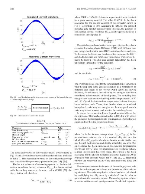
Fig. 14.<br />
Illustration <strong>of</strong> a converter model.<br />
TABLE II<br />
CONSTRAINTS AND CONDITIONS FOR CONVERTER OPTIMIZATION<br />
The inputs and outputs <strong>of</strong> the converter model are illustrated in<br />
Fig. 14 and all optimization constraints and conditions are listed<br />
in Table II. This optimization based on the semiconductor chip<br />
area is motivated by previously presented works [25], [26].<br />
The thermal resistance <strong>of</strong> the cooling system, i.e., the heat sink<br />
surface to ambient thermal resistance R th,sa , has been modeled<br />
with the cooling system per<strong>for</strong>mance index (CSPI) [27]; the<br />
R th,sa is then calculated as<br />
R th,sa =<br />
1<br />
CSPI · V CS<br />
(16)<br />
A T =0.95 mm2<br />
A · I N +3.2 mm 2 (18)<br />
and <strong>for</strong> the diode<br />
A D =0.47 mm2<br />
A · I N +3.6 mm 2 . (19)<br />
The switching losses scaled to the same current do not vary much<br />
with the chip size in the considered range, as a comparison <strong>of</strong><br />
different data sheets <strong>of</strong> the selected IGBT series has shown;<br />
there<strong>for</strong>e, <strong>for</strong> this study, the switching loss energies have been<br />
considered as independent <strong>of</strong> the chip area. The switching loss<br />
energies have been extracted at two junction temperatures (25 ◦ C<br />
and 150 ◦ C) and, <strong>for</strong> intermediate temperatures, a linear interpolation<br />
has been made. These, from the data sheet extracted and<br />
interpolated, switching loss energies are then assigned to each<br />
switching instant in order to determine the switching losses.<br />
In return, the conduction losses depend substantially on the<br />
chip size area. This has been modeled as in [26], but with taking<br />
the impact <strong>of</strong> the temperature into consideration. The following<br />
equation describes the conduction losses<br />
P cond (A, i, T j,T /D )=V f · i + R on,N(T j,T /D ) · A N<br />
· i 2<br />
A<br />
(20)<br />
where V f is the <strong>for</strong>ward voltage drop, R on,N (T j,T /D ) is the<br />
nominal on-resistance, A N is the nominal chip size area (to<br />
which R on,N (T j,T /D ) is taken from the data sheet), i is the current<br />
through the transistor, and A is the actual chip size area. The<br />
on-resistance has been extracted at two junction temperatures<br />
(25 ◦ C and 150 ◦ C) and, <strong>for</strong> intermediate on-resistance values,<br />
a linear interpolation has been made. The current i has been<br />
calculated <strong>for</strong> the chosen modulation scheme. Equation (20) is<br />
evaluated with different values <strong>for</strong> V f and R on,N , depending<br />
whether the conduction losses <strong>of</strong> the transistor or the diode are<br />
calculated.<br />
The converter volume is the sum <strong>of</strong> the cooling system volume,<br />
the dc-link capacitor volume, and the volume <strong>of</strong> the switching<br />
devices. The switching device volume has been calculated<br />
by multiplying the chip areas by a depth <strong>of</strong> 1 cm in order to<br />
approximate the transistor volume. The cooling system volume<br />
is known as it is a model input parameter. The dc-link capacitor