Optimal Design of LCL Harmonic Filters for Three-Phase PFC ...
Optimal Design of LCL Harmonic Filters for Three-Phase PFC ...
Optimal Design of LCL Harmonic Filters for Three-Phase PFC ...

Create successful ePaper yourself
Turn your PDF publications into a flip-book with our unique Google optimized e-Paper software.
MÜHLETHALER et al.: OPTIMAL DESIGN OF <strong>LCL</strong> HARMONIC FILTERS FOR THREE-PHASE <strong>PFC</strong> RECTIFIERS 3121<br />
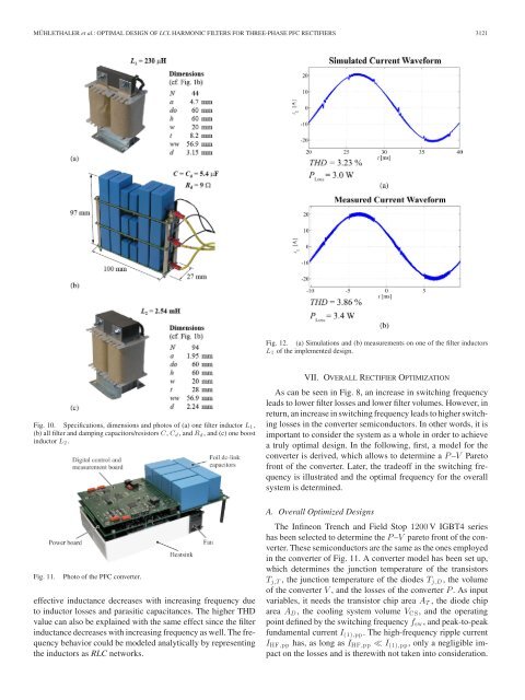
Fig. 12. (a) Simulations and (b) measurements on one <strong>of</strong> the filter inductors<br />
L 1 <strong>of</strong> the implemented design.<br />
Fig. 10. Specifications, dimensions and photos <strong>of</strong> (a) one filter inductor L 1 ,<br />
(b) all filter and damping capacitors/resistors C, C d ,andR d , and (c) one boost<br />
inductor L 2 .<br />
VII. OVERALL RECTIFIER OPTIMIZATION<br />
As can be seen in Fig. 8, an increase in switching frequency<br />
leads to lower filter losses and lower filter volumes. However, in<br />
return, an increase in switching frequency leads to higher switching<br />
losses in the converter semiconductors. In other words, it is<br />
important to consider the system as a whole in order to achieve<br />
a truly optimal design. In the following, first, a model <strong>for</strong> the<br />
converter is derived, which allows to determine a P –V Pareto<br />
front <strong>of</strong> the converter. Later, the trade<strong>of</strong>f in the switching frequency<br />
is illustrated and the optimal frequency <strong>for</strong> the overall<br />
system is determined.<br />
Fig. 11.<br />
Photo <strong>of</strong> the <strong>PFC</strong> converter.<br />
effective inductance decreases with increasing frequency due<br />
to inductor losses and parasitic capacitances. The higher THD<br />
value can also be explained with the same effect since the filter<br />
inductance decreases with increasing frequency as well. The frequency<br />
behavior could be modeled analytically by representing<br />
the inductors as RLC networks.<br />
A. Overall Optimized <strong>Design</strong>s<br />
The Infineon Trench and Field Stop 1200 V IGBT4 series<br />
has been selected to determine the P –V pareto front <strong>of</strong> the converter.<br />
These semiconductors are the same as the ones employed<br />
in the converter <strong>of</strong> Fig. 11. A converter model has been set up,<br />
which determines the junction temperature <strong>of</strong> the transistors<br />
T j,T , the junction temperature <strong>of</strong> the diodes T j,D ,thevolume<br />
<strong>of</strong> the converter V , and the losses <strong>of</strong> the converter P . As input<br />
variables, it needs the transistor chip area A T , the diode chip<br />
area A D , the cooling system volume V CS , and the operating<br />
point defined by the switching frequency f sw , and peak-to-peak<br />
fundamental current I (1),pp . The high-frequency ripple current<br />
I HF,pp has, as long as I HF,pp ≪ I (1),pp , only a negligible impact<br />
on the losses and is therewith not taken into consideration.