The Characteristics of a Dual-Layer Optical Disk with Read-Only and ...
The Characteristics of a Dual-Layer Optical Disk with Read-Only and ...
The Characteristics of a Dual-Layer Optical Disk with Read-Only and ...

Create successful ePaper yourself
Turn your PDF publications into a flip-book with our unique Google optimized e-Paper software.
IEEE JOURNAL OF SELECTED TOPICS IN QUANTUM ELECTRONICS, VOL. 4, NO. 5, SEPTEMBER/OCTOBER 1998 821<br />
<strong>The</strong> <strong>Characteristics</strong> <strong>of</strong> a <strong>Dual</strong>-<strong>Layer</strong> <strong>Optical</strong> <strong>Disk</strong><br />
<strong>with</strong> <strong>Read</strong>-<strong>Only</strong> <strong>and</strong> Erasable Functions<br />
Bor-Wen Yang <strong>and</strong> Han-Ping D. Shieh<br />
Abstract—A dual-layer optical disk comprised <strong>of</strong> a read-only<br />
layer <strong>and</strong> a phase-change layer was designed to perform the<br />
read-only <strong>and</strong> erasable dual-functionality in an optical disk. With<br />
the properly designed dual-layer disk structure, 23 mW <strong>of</strong> write<br />
power was adequate to write data marks on the erasable phasechange<br />
layer; simultaneously, equal magnitude <strong>of</strong> sufficient radi<strong>of</strong>requency<br />
readout signals could be obtained on both its data<br />
layers. <strong>The</strong> analyzes <strong>of</strong> its recording characteristics demonstrated<br />
the feasibility <strong>of</strong> the dual-functional optical disk.<br />
Index Terms— <strong>Dual</strong>-functional optical disk, dual-layer optical<br />
disk, interlayer crosstalk, optical disk.<br />
I. INTRODUCTION<br />
OPTICAL DISKS consisting <strong>of</strong> multiple data layers were<br />
proposed to multiply the recording density by volumetric<br />
optical storage [1]. A number <strong>of</strong> multilayer optical disk<br />
structures were suggested for higher density storage applications<br />
[2]–[6]. For example, two embodiments <strong>of</strong> dual-layer<br />
read-only optical disk announced by Philips/Sony <strong>and</strong> 3M<br />
companies became the pioneers <strong>of</strong> dual-layer digital versatile<br />
disk–read-only memory (DVD-ROM) [3], [4]. <strong>The</strong>reafter,<br />
constructions <strong>of</strong> dual-layer write-once read-many (WORM)<br />
optical disks were devised by applying nonreversible phasechange<br />
material or dye mixture, respectively [5], [6], so that<br />
volumetric optical storage technology could be extended to the<br />
world <strong>of</strong> recordable data recording.<br />
On the contrary, it requires more effort to contrive a duallayer<br />
digital versatile disk–r<strong>and</strong>om access memory (DVD-<br />
RAM) composed <strong>of</strong> two reversible data layers. In general,<br />
the upper data layer which is the first data layer defined to<br />
be the laser incident side layer <strong>of</strong> a dual-layer optical disk<br />
is designed to be semitransparent to make the lower data<br />
layer which is the second data layer accessible [7]; however,<br />
due to the requirement <strong>of</strong> metallic cooling layer for high<br />
speed thermal recording <strong>and</strong> temperature descending [8], the<br />
currently available erasable media, including magnetooptical<br />
or phase-change, have not sufficient transmissivity to be the<br />
semireflective layer. This is one <strong>of</strong> the important issues why a<br />
reliable dual-layer DVD-RAM is still challenging nowadays.<br />
To resolve the problem, a semireflective read-only layer <strong>with</strong><br />
sufficient transmissivity is proposed to replace the upper RAM<br />
Manuscript received March 17, 1998; revised June 29, 1998. This work<br />
was supported by National Science Council <strong>of</strong> the Republic <strong>of</strong> China under<br />
Contract NSC 86-2622-L009-002.<br />
<strong>The</strong> authors are <strong>with</strong> Institute <strong>of</strong> Electro-<strong>Optical</strong> Engineering, National<br />
Chiao Tung University, Hsinchu 30050, Taiwan, R.O.C.<br />
Publisher Item Identifier S 1077-260X(98)08530-X.<br />
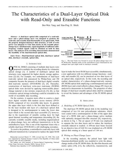
Fig. 1. <strong>The</strong> laser beam was focused to access the phase-change layer <strong>of</strong> a<br />
PC-ROM disk. R<strong>and</strong>om marks on the semireflective layer illuminated by the<br />
enlarged laser spot might result in interlayer crosstalk.<br />
layer to make the lower RAM layer accessible; simultaneously,<br />
a new application <strong>with</strong> two different storage functions—readonly<br />
<strong>and</strong> erasable [9], can be practiced on two data layers <strong>of</strong><br />
an optical disk, respectively. In this work, the recording <strong>and</strong><br />
readout characteristics <strong>of</strong> a phase-change/read-only memory<br />
(PC-ROM) optical disk employing a semitransparent read-only<br />
(ROM) layer <strong>and</strong> a total-reflective phase-change (PC) layer are<br />
analyzed to demonstrate its feasibility. <strong>The</strong> properties <strong>of</strong> other<br />
designs <strong>of</strong> dual-layer erasable optical disks shall be compared<br />
to reveal the features <strong>and</strong> advantages <strong>of</strong> the PC-ROM optical<br />
disk.<br />
II. SIMULATION<br />
A. Modeling <strong>of</strong> PC-ROM <strong>Optical</strong> <strong>Disk</strong>s<br />
<strong>The</strong> dual-layer PC-ROM optical disk in the modeling was<br />
comprised <strong>of</strong> two 0.6 mm polycarbonate substrates, which<br />
were coated <strong>with</strong> a semitransparent Al film <strong>of</strong> the upper data<br />
layer <strong>of</strong> a ROM disk <strong>and</strong> a phase-change active medium<br />
<strong>with</strong> optimally designed thin-film structure [8], respectively,<br />
as shown in Fig. 1. <strong>The</strong> air spacer <strong>of</strong> 50 mm was employed<br />
to separate the two data layers <strong>and</strong> to reduce the interlayer<br />
crosstalk induced in readout. A 650-nm laser beam focused<br />
by an objective lens <strong>of</strong> 0.60 NA was irradiated on a PC-ROM<br />
optical disk rotating at a linear speed <strong>of</strong> 3.84 m/s.<br />
B. Writing on Phase-Change <strong>Layer</strong><br />
In the recording analysis, the pulsed laser light <strong>with</strong><br />
Gaussian-distributed pr<strong>of</strong>ile was modeled to write the phasechange<br />
media <strong>of</strong> the PC-ROM disks. By thin-film theorem <strong>and</strong><br />
metric optics [10], [11], the reflectivity, transmissivity, <strong>and</strong><br />
1077–260X/98$10.00 © 1998 IEEE
822 IEEE JOURNAL OF SELECTED TOPICS IN QUANTUM ELECTRONICS, VOL. 4, NO. 5, SEPTEMBER/OCTOBER 1998<br />
absorption coefficient <strong>of</strong> the two data layers were calculated by<br />
(1)<br />
where the <strong>and</strong> represent the optical admittances [11]<br />
<strong>of</strong> the input <strong>and</strong> output thin-film medium, respectively; the<br />
<strong>and</strong> denote the matrix elements <strong>of</strong> the resultant product <strong>of</strong><br />
all relating thin-film optical matrices, respectively; the signs<br />
<strong>of</strong> asterisk are added to terms on which the complex<br />
conjugates are taken. <strong>The</strong> temperature rising <strong>and</strong> descending<br />
process effectuated by the laser spot irradiated on the phasechange<br />
layer was analyzed by the dynamic heat diffusion<br />
equation [12]. <strong>The</strong> writing pulses were applied to heat the<br />
phase-change layer above its melting point ( 600 C) to<br />
record amorphous data marks on it. Reasonable write power<br />
<strong>of</strong> about 23 mW shall be proved to be sufficient to record<br />
reliable data marks on the phase-change layer through the<br />
semitransparent read-only data layer.<br />
C. Modeling <strong>of</strong> RF <strong>Read</strong>out Signal <strong>and</strong> Interlayer Crosstalk<br />
<strong>The</strong> RF readout signals detected from both data layers were<br />
derived from the readout modeling, so that the optimal disk<br />
structure <strong>with</strong> balanced readout on both data layers could be<br />
designed. To derive the RF readout signals, the DC readout<br />
laser beam <strong>with</strong> Gaussian pr<strong>of</strong>ile was first modeled. <strong>The</strong>n, the<br />
read-only <strong>and</strong> phase-change data marks were simulated on the<br />
corresponding data layers, respectively, by a series <strong>of</strong> r<strong>and</strong>om<br />
phase pits <strong>and</strong> amorphous data marks. Eventually, the optical<br />
energy detected by the objective lens reflected from the<br />
focused data layer was derived by taking the convolution <strong>of</strong><br />
the diffraction-limited spot <strong>and</strong> the irradiated data marks, as<br />
shown in Fig. 2:<br />
where the denotes the Gaussian energy distribution<br />
<strong>of</strong> the laser spot; is a function which describes the<br />
reflectivity distribution <strong>of</strong> the read-only or phase-change data<br />
surfaces. On the read-only layer, the reflectivity difference<br />
exists between the embossed data marks <strong>and</strong> the l<strong>and</strong> area; on<br />
the phase-change layer, the reflectivity difference is induced by<br />
the amorphous data marks <strong>and</strong> the unrecorded crystalline area.<br />
When the phase-change layer is read out, the semireflective<br />
layer shall reflect back part <strong>of</strong> the laser beam, which may<br />
couple into the readout channel <strong>and</strong> induce interlayer crosstalk.<br />
Besides the diffraction-limited laser spot focused on the totalreflective<br />
layer, an enlarged laser spot is generated on the<br />
semireflective layer; hundreds <strong>of</strong> data marks recorded on this<br />
out-<strong>of</strong>-focus layer are simultaneously illuminated <strong>and</strong> read out,<br />
thus result in interlayer crosstalk [13].<br />
It is essential to reduce interlayer crosstalk in designing<br />
a dual-layer optical disk because it shall degrade the RF<br />
signal <strong>and</strong> deteriorate the readout contrast [13]. By the readout<br />
(2)<br />
Fig. 2. <strong>The</strong> RF readout signal <strong>of</strong> a PC-ROM optical disk was derived by<br />
the convolution <strong>of</strong> the focused laser spot <strong>with</strong> the data marks recorded on<br />
either data layer.<br />
TABLE I<br />
OPTICAL AND THERMAL PARAMETERS OF THE<br />
MATERIALS USED IN THE PC-ROM OPTICAL DISKS<br />
modeling, the interlayer crosstalk could likewise be derived<br />
by taking the convolution <strong>of</strong> the enlarged laser pr<strong>of</strong>ile <strong>and</strong> the<br />
reflectivity distribution <strong>of</strong> the out-<strong>of</strong>-focus data surface. <strong>The</strong><br />
disk structure <strong>of</strong> a PC-ROM shall be optimized by suppressing<br />
the interlayer crosstalk induced in readout.<br />
III. RECORDING ON PHASE-CHANGE LAYER<br />
To write the phase-change layer <strong>of</strong> the PC-ROM, the laser<br />
power needs to be properly increased to compensate the optical<br />
energy lost in transmitting through the semireflective layer.<br />
<strong>The</strong> optical <strong>and</strong> thermal parameters <strong>of</strong> the materials used in<br />
the PC-ROM’s in the recording simulation are listed in Table I<br />
[8]. By the thermal modeling, the phase-change layer can<br />
be locally heated to record amorphous marks <strong>of</strong> about 0.35<br />
mm by 12-mW laser beam <strong>of</strong> 80-ns pulse duration (writing<br />
frequency MHz, <strong>and</strong> duty cycle %) in absence<br />
<strong>of</strong> the semireflective layer, as shown in Fig. 3(a). However,<br />
if the 12-mW laser pulse is irradiated onto a PC-ROM disk<br />
<strong>with</strong> a 25-Å-thick semireflective layer <strong>of</strong> the upper ROM disk,<br />
as shown in Fig. 3(b), only about 5 mW <strong>of</strong> laser power can<br />
transmit through the semireflective layer, thus fails to write on<br />
the phase-change layer. Larger portion <strong>of</strong> the energy loss is<br />
caused by optical absorption rather than optical reflection on<br />
the semireflective film, which is indicated by the absorption<br />
coefficient <strong>and</strong> reflectivity <strong>of</strong> the semireflective film,<br />
as shown in Fig. 4. Have the write power increased to 23 mW,<br />
data marks <strong>of</strong> about 0.35 mm can now be recorded on the<br />
lower data layer <strong>of</strong> the phase-change layer <strong>of</strong> the PC-ROM<br />
disk <strong>with</strong> a 25-Å-thick semireflector, as shown in Fig. 3(c).<br />
<strong>The</strong> thicker the semireflective layer is, the less optical energy<br />
the phase-change layer receives, <strong>and</strong> thus the higher effective<br />
write power is required.
YANG et al.: THE CHARACTERISTICS OF A DUAL-LAYER OPTICAL DISK 823<br />
Fig. 3. <strong>The</strong> amorphous marks recorded on the phase-change layer <strong>of</strong> the<br />
PC-ROM optical disks <strong>with</strong> different thickness <strong>of</strong> semireflectors (t) <strong>and</strong> write<br />
powers (Pw).<br />
Fig. 5. <strong>The</strong> normalized RF signal (F signal ) <strong>and</strong> interlayer crosstalk (Fxtalk)<br />
<strong>of</strong> PC-ROM disks derived in two readout modes, as a function <strong>of</strong> semireflector<br />
thickness.<br />
Fig. 4. <strong>The</strong> absorption coefficient (A), the reflectivity (R) <strong>of</strong> the semireflective<br />
layer, <strong>and</strong> the write power (Pw) required to record signals on a PC-ROM<br />
disk, as a function <strong>of</strong> semireflector thickness.<br />
IV. READOUT ON BOTH DATA LAYERS<br />
<strong>The</strong>re are two modes in reading a PC-ROM optical disk: for<br />
example, the laser beam is focused to read the lower data layer<br />
<strong>of</strong> the phase-change layer in mode-1, <strong>and</strong> to read the upper data<br />
layer <strong>of</strong> the read-only layer in mode-2. To preclude the effect<br />
<strong>of</strong> magnitude <strong>of</strong> the read power in the readout modeling, the<br />
RF signal (or interlayer crosstalk is normalized<br />
by dividing the read power carrying the RF readout signal (or<br />
interlayer crosstalk) by the incident read power.<br />
By readout analyzes on both data layers, the disk structure<br />
<strong>of</strong> a PC-ROM is optimized by suppressing the interlayer<br />
crosstalk induced in readout. In read mode-1, the is<br />
proportional to <strong>and</strong> the is proportional<br />
to to the first-order approximation, where the<br />
<strong>and</strong> denote the transmissivity <strong>of</strong> semireflective layer, the<br />
reflectivity <strong>of</strong> total-reflective layer <strong>and</strong> semireflective layer,<br />
respectively; contrarily, in mode-2 to read the read-only layer,<br />
the is proportional to <strong>and</strong> the is proportional<br />
to as shown by the curves depicted in Fig. 5.<br />
In reading the phase-change layer, a semireflective layer too<br />
much thicker than 25 Å (the intersection value <strong>of</strong> the<br />
<strong>and</strong> curves) blocks the read beam incident to the phasechange<br />
layer, thus derives insufficient RF signal to compete<br />
<strong>with</strong> the interlayer crosstalk noise. On the contrary, a PC-ROM<br />
disk <strong>with</strong> semireflective film too much thinner than 25 Åis<br />
not suitable for readout on the ROM layer, since large part<br />
(a)<br />
(b)<br />
Fig. 6. <strong>The</strong> simulated RF signal in reading (a) phase-change <strong>and</strong> (b) ROM<br />
layers <strong>of</strong> a PC-ROM disk <strong>with</strong> a 25-Å-thick semireflective layer.<br />
<strong>of</strong> laser energy is leaked to the phase-change layer to derive<br />
interlayer crosstalk more intense than the RF signal. Thus, the<br />
thickness <strong>of</strong> semireflective layer is optimally designed around<br />
25 Å to suppress interlayer crosstalk in readout.<br />
Due to the existence <strong>of</strong> semireflective layer, the RF signal<br />
magnitude derived from either data layer may be distinct from<br />
the other, thereby results in unbalanced readout, which leads<br />
to difficulty in design <strong>of</strong> readout electronics [2]. Balanced RF<br />
signals were achieved on the optimized structure <strong>with</strong> a 25-Åthick<br />
semireflector because the normalized RF signal Fsignal<br />
<strong>of</strong> read mode 1 is just identical to that <strong>of</strong> read mode 2 at the<br />
intersection point, as shown in Fig. 5.<br />
To derive the RF readout signal in unit <strong>of</strong> volts, the detection<br />
channel (from the objective lens to the optical detector) is<br />
modeled as a linear system, so that the RF readout signal (in<br />
volts) extracted from the optical detector can be derived by<br />
the readout optical energy detected by the objective lens.<br />
<strong>The</strong> measured RF signal <strong>of</strong> a conventional CD is used as a<br />
st<strong>and</strong>ard to characterize the detection channel to transform the<br />
inputted to the outputted RF signal amplitude in volts.<br />
By this way, the RF signal <strong>of</strong> the phase-change layer <strong>of</strong> a PC-
824 IEEE JOURNAL OF SELECTED TOPICS IN QUANTUM ELECTRONICS, VOL. 4, NO. 5, SEPTEMBER/OCTOBER 1998<br />
(a) (b) (c)<br />
Fig. 7. <strong>The</strong> possible three designs <strong>of</strong> erasable dual-layer optical disks <strong>and</strong> the corresponding RF readout signal (F signal ; such as F ROM ,F RAM ,F RAM1 ,<br />
<strong>and</strong> F RAM2 ) as a function <strong>of</strong> semireflector thickness (t, such as t ROM , t RAM , <strong>and</strong> t RAM1 ). (a) PC-ROM. (b) <strong>Dual</strong>-layer disk <strong>with</strong> a semireflective RAM<br />
layer <strong>and</strong> a total-reflective ROM layer. (c) <strong>Dual</strong>-layer DVD-RAM.<br />
ROM disk <strong>with</strong> a 25-Å-thick semireflective layer was derived,<br />
as shown in Fig. 6(a), where the peak signals were derived by<br />
the crystalline area <strong>with</strong> higher reflectivity, while the valley<br />
levels were by the amorphous marks recorded by 23 mW <strong>of</strong><br />
80-ns laser pulse, as shown in Fig. 3(c); similar magnitude<br />
<strong>of</strong> RF signal in r<strong>and</strong>om data sequence was derived from the<br />
read-only layer <strong>of</strong> the PC-ROM disk, as shown in Fig. 6(b),<br />
where the peak signal levels were derived by the l<strong>and</strong> area<br />
<strong>with</strong> higher reflectivity, while the valley levels was derived by<br />
the concave r<strong>and</strong>om data marks. Thus, <strong>with</strong> the semireflective<br />
film coated around 25 Å, balanced RF readout signals are<br />
derived from both data layers <strong>of</strong> the PC-ROM disk, which can<br />
effectively simplify the design <strong>of</strong> readout electronics.<br />
V. DISCUSSION<br />
<strong>The</strong> recording/readout characteristics <strong>of</strong> possible designs <strong>of</strong><br />
dual-layer optical disks <strong>with</strong> recording function were examined<br />
to reveal the advantages <strong>of</strong> PC-ROM. <strong>The</strong> optimized PC-ROM<br />
optical disk, as shown in Fig. 7(a), is <strong>with</strong> merits <strong>of</strong> balanced<br />
readout <strong>and</strong> reasonable power requirement, as described above.<br />
A dual-layer optical disk <strong>with</strong> a semireflective RAM layer <strong>and</strong><br />
a total-reflective ROM layer is shown in Fig. 7(b). Due to<br />
the requirement <strong>of</strong> sufficient optical absorption <strong>and</strong> reflection<br />
for writing <strong>and</strong> readout, the transmissivity <strong>of</strong> the RAM layer<br />
is in general less than 10% [8], [14], so that the totalreflective<br />
ROM layer <strong>of</strong> this dual-layer optical disk is hardly<br />
detectable. Accordingly, by readout simulation, the RF signal<br />
derived from the ROM layer <strong>of</strong> the disk was much lower<br />
than that <strong>of</strong> the semireflective RAM layer, thus the balanced<br />
readout was hard to be achieved. <strong>The</strong> similar issue exists in<br />
a dual-layer DVD-RAM, as shown in Fig. 7(c). Moreover,<br />
by recording simulation, the blocking effect <strong>of</strong> the upper<br />
RAM layer drastically increases the power required to write<br />
the lower RAM layer <strong>of</strong> the dual-layer DVD-RAM, typically<br />
larger than 35 mW.<br />
<strong>The</strong> dual-layer PC-ROM optical disk is promising to be<br />
put into practice since its significant features, such as low<br />
write power <strong>and</strong> balanced readout, remains almost unchanged<br />
under the presence <strong>of</strong> significant fabrication variance. <strong>The</strong><br />
degree <strong>of</strong> readout unbalance (the readout unbalance factor)<br />
is defined as the higher RF signal derived from one <strong>of</strong> the<br />
data layers divided by that <strong>of</strong> the lower signal derived from<br />
the other. <strong>The</strong> factor is thus always larger than or equals unity,<br />
Fig. 8. <strong>The</strong> readout unbalance factor <strong>and</strong> write power for a PC-ROM disk<br />
as a function <strong>of</strong> semireflective layer thickness. <strong>The</strong> semireflector thickness <strong>of</strong><br />
the shaded area is (2565%) Å.<br />
wherein the balanced readout is achieved when the factor<br />
equals 1.0. By the recording <strong>and</strong> readout analyzes described<br />
above, the write power <strong>and</strong> the readout unbalance factor <strong>of</strong><br />
the optimized PC-ROM disk <strong>with</strong> a 25-Å-thick semireflector<br />
were 23 mW <strong>and</strong> 1.0, respectively, as illustrated in Fig. 8.<br />
An assumed manufacturing variance <strong>of</strong> semireflector thickness<br />
<strong>of</strong> 5% at the nominal value <strong>of</strong> 25 Å still keeps the write<br />
power requirement <strong>and</strong> readout balance factor below 24 mW<br />
<strong>and</strong> 1.2, respectively, which is capable <strong>of</strong> accommodating to<br />
today’s diode laser [15] <strong>and</strong> signal process 1 technologies. Too<br />
large power requirement <strong>and</strong>/or too high readout unbalance<br />
factor are among the main factors to prohibit the dual-layer<br />
erasable optical disks, as shown in Fig. 7(b) or (c), from being<br />
practicable nowadays.<br />
VI. CONCLUSION<br />
<strong>The</strong> recording <strong>and</strong> readout characteristics <strong>of</strong> a dualfunctional<br />
PC-ROM optical disk were analyzed to demonstrate<br />
its feasibility. <strong>The</strong> PC-ROM disk was optimized <strong>with</strong> a<br />
semireflective layer <strong>of</strong> around 25 Å thick to suppress the<br />
interlayer crosstalk. Data recording on the phase-change layer<br />
<strong>of</strong> the optimal PC-ROM disk is achieved at reasonable write<br />
power <strong>of</strong> about 23 mW; simultaneously, balanced readout<br />
on both data layers can be acquired. A fabrication tolerance<br />
<strong>of</strong> semireflector thickness <strong>of</strong> 5% is allowable for the PC-<br />
ROM disk since it will not induce significant writing or<br />
1 <strong>The</strong> Compact <strong>Disk</strong>-<strong>Read</strong> <strong>Only</strong> Memory (CD-ROM) red book.
YANG et al.: THE CHARACTERISTICS OF A DUAL-LAYER OPTICAL DISK 825<br />
readout characteristics variation. Newly developed phasechange<br />
materials or structures <strong>with</strong> sufficient transmissivity<br />
may exp<strong>and</strong> the varieties in design <strong>of</strong> multilayer optical disks;<br />
however, owing to the temporary lack <strong>of</strong> erasable media <strong>with</strong><br />
high enough transmissivity to be the semireflective layer <strong>of</strong><br />
a dual-layer DVD-RAM, the PC-ROM optical disk is well<br />
promising to practice read-only <strong>and</strong> erasable dual functions.<br />
[14] Y. Murakami, J. Nakayama, M. Mieda, A. Takahashi, K. Ohta, <strong>and</strong> K.<br />
Shigematsu, “Precise mark shape control in mark length recording on<br />
magnetooptical disk,” Jpn. J. Appl. Phys., vol. 32, pp. 5342–5348, 1993.<br />
[15] A. Shima, H. Tada, K. Ono, M. Fujiwara, T. Utakouji, T. Kimura,<br />
M. Takemi, <strong>and</strong> H. Higuchi, “Highly reliable 60-degrees-C 50-mW<br />
operation <strong>of</strong> 650-nm b<strong>and</strong> window-mirror laser-diodes,” IEEE Photon.<br />
Technol. Lett., vol. 9, pp. 413–415, 1997.<br />
REFERENCES<br />
[1] P. G. Wohimut <strong>and</strong> F. D. Neu, “Three dimensional electro-optical<br />
retrieval system,” U.S. Patent 3 946 367.<br />
[2] P. L. Holster <strong>and</strong> J. M. Wittkamper, “Multilayer information disc,” U.S.<br />
Patent 4 450 553.<br />
[3] “Philips <strong>and</strong> Sony propose specifications for high density multimedia<br />
compact disc,” press release, Dec. 1994.<br />
[4] “3M announces dual-layer construction process for high-density CD-<br />
ROM,” 3M News, Nov. 1994.<br />
[5] W. I. Imaino, H. J. Rosen, K. A. Rubin, <strong>and</strong> W. W.-C. Tang, “<strong>Optical</strong><br />
data storage system <strong>with</strong> multiple write-once phase-change recording<br />
layers,” U.S. Patent 5 555 537.<br />
[6] H. J. Rosen, K. A. Rubin, <strong>and</strong> W. W.-C. Tang, “<strong>Optical</strong> disk data storage<br />
system <strong>with</strong> multiple write-once dye-based data layers,” U.S. Patent<br />
5 627 817.<br />
[7] J. Isailovic, in SPIE Proc. <strong>Optical</strong> Storage <strong>and</strong> Scanning Tech., 1989,<br />
vol. 1139, pp. 155–160.<br />
[8] T. Ohta, K. Inoue, M. Uchida, K. Yoshioka, T. Akiyama, S. Furukawa,<br />
K. Nagata, <strong>and</strong> S. Nakamura, “Phase change disk media having rapid<br />
cooling structure,” Jpn. J. Appl. Phys., vol. 28, supp. 28-3, pp. 123–128,<br />
1989.<br />
[9] K. Nishiuchi, K. Nagata, <strong>and</strong> N. Akahira, “<strong>Dual</strong>-layer optical disk <strong>with</strong><br />
phase change rewritable <strong>and</strong> read only layers,” in Extended Abstracts,<br />
56th Autumn Meet., 1995, Jpn. Soc. Appl. Phys., 1995, p. 959 (in<br />
Japanese).<br />
[10] A. Yariv, <strong>Optical</strong> Electronics. New York: Saunders College Publishing,<br />
1991.<br />
[11] H. A. Macleod, Thin-Film <strong>Optical</strong> Filters. New York: McGraw-Hill,<br />
1990.<br />
[12] M. Mansuripur <strong>and</strong> G. A. N. Connell, “Laser-induced local heating <strong>of</strong><br />
moving multilayer media,” Appl. Opt., vol. 22, pp. 666–670, 1983.<br />
[13] B.-W. Yang <strong>and</strong> H.-P. D. Shieh, “Interlayer crosstalk in dual-layer<br />
read-only optical disks,” Appl. Opt., to be published.<br />
Bor-Wen Yang was born in Hsinchu, Taiwan,<br />
R.O.C. He received the B.Sc. degree in electrophysics<br />
from National Chiao Tung University,<br />
Hsinchu, Taiwan, Republic <strong>of</strong> China, in 1992, where<br />
he is currently working toward the Ph.D. degree at<br />
the Institute <strong>of</strong> Electro-<strong>Optical</strong> Engineering.<br />
He has worked in the field <strong>of</strong> optical storage for<br />
a couple <strong>of</strong> years, <strong>and</strong> his main interests are in the<br />
analyses <strong>of</strong> recording <strong>and</strong> readout characteristics <strong>of</strong><br />
multilayer optical disks.<br />
Han-Ping David Shieh received the B.Sc. degree<br />
in physics from National Taiwan University, Taipei,<br />
Taiwan, R.O.C., in 1975, the M.Sc. degree in electrical<br />
engineering from the Ohio State University,<br />
Columbus, OH, in 1980, <strong>and</strong> the Ph.D. degree<br />
from Carnegie Mellon University, Pittsburgh, PA,<br />
in 1987.<br />
Since 1988, he has been a Research Staff Member<br />
in IBM Research Division, T. J. Watson Research<br />
Center, <strong>and</strong> Adjunct Assistant Pr<strong>of</strong>essor <strong>of</strong> Department<br />
<strong>of</strong> Electrical <strong>and</strong> Computer Engineering,<br />
Carnegie Mellon University, Pittsburgh, PA. Since 1992, he has been a<br />
Pr<strong>of</strong>essor <strong>of</strong> the Institute <strong>of</strong> Electro-Optic Engineering <strong>and</strong> Microelectronics<br />
<strong>and</strong> Information Research Center, National Chiao Tung University, Hsinchu,<br />
Taiwan, R.O.C. He has worked in the field <strong>of</strong> optical storage for over ten<br />
years, <strong>and</strong> his main interests now are the technologies <strong>of</strong> optical data storage<br />
<strong>and</strong> flat-panel display.