Compact CPW-MS-CPW Two-Stage pHEMT Amplifier ... - IEEE Xplore
Compact CPW-MS-CPW Two-Stage pHEMT Amplifier ... - IEEE Xplore
Compact CPW-MS-CPW Two-Stage pHEMT Amplifier ... - IEEE Xplore

You also want an ePaper? Increase the reach of your titles
YUMPU automatically turns print PDFs into web optimized ePapers that Google loves.
112 <strong>IEEE</strong> MICROWAVE AND WIRELESS COMPONENTS LETTERS, VOL. 18, NO. 2, FEBRUARY 2008<br />
<strong>Compact</strong> <strong>CPW</strong>-<strong>MS</strong>-<strong>CPW</strong> <strong>Two</strong>-<strong>Stage</strong> <strong>pHEMT</strong><br />
<strong>Amplifier</strong> Compatible With Flip Chip<br />
Technique in V-Band Frequencies<br />
Jen-Yi Su, Student Member, <strong>IEEE</strong>, Chinchun Meng, Member, <strong>IEEE</strong>, Yueh-Ting Lee, and Guo-Wei Huang<br />
Abstract—The V-band coplanar waveguide (<strong>CPW</strong>)–microstrip<br />
line (<strong>MS</strong>)–<strong>CPW</strong> two-stage amplifier with the flip-chip bonding<br />
technique is demonstrated using 0.15 m AlGaAs/InGaAs pseudomorphic<br />
high electron mobility transistor technology. The <strong>CPW</strong><br />
is used at input and output ports for flip-chip assemblies and the<br />
<strong>MS</strong> transmission line is employed in the interstage to reduce chip<br />
size. This two-stage amplifier employs transistors as the <strong>CPW</strong>–<strong>MS</strong><br />
transition and the <strong>MS</strong>–<strong>CPW</strong> transition in the first stage and the<br />
second stage, respectively. The <strong>CPW</strong>–<strong>MS</strong>–<strong>CPW</strong> two-stage amplifier<br />
has a gain of 14.8 dB, input return loss of 10 dB and output<br />
return loss of 22 dB at 53.5 GHz. After the flip-chip bonding, the<br />
measured performances have almost the same value.<br />
Index Terms—Coplanar waveguide (<strong>CPW</strong>), flip-chip bonding,<br />
microstrip line (<strong>MS</strong>), pseudomorphic high electron mobility transistor<br />
(<strong>pHEMT</strong>).<br />
I. INTRODUCTION<br />
RECENTLY, the flip-chip bonding technique is necessary<br />
for packages of millimeter-wave monolithic microwave<br />
integrated circuits (MMICs) [1]–[5]. The flip-chip bonding<br />
technique has advantages over traditional wire bonding<br />
technique because of the shorter interconnect path, better<br />
mechanical stability, higher reliability and less parasitic effects<br />
[1]–[3]. Coplanar waveguide (<strong>CPW</strong>) topology [1], [2], [6] is<br />
widely employed in the millimeter-wave flip-chip MMICs<br />
to provide a smooth electric transition interface between the<br />
chip and the substrate carrier while the microstrip line (<strong>MS</strong>)<br />
topology after flip-chip assemblies shows a strong gain degradation<br />
for the frequencies above 50 GHz [5] even though the<br />
layout of an <strong>MS</strong>-type topology can save much real estate in<br />
the IC technology. The <strong>CPW</strong> MMIC has less complicated<br />
processing steps by eliminating via hole etching, wafer thinning,<br />
and backside processing in the <strong>MS</strong>-type process [1], [5].<br />
Although the <strong>CPW</strong> circuit has the advantage of simple process,<br />
the lower effective dielectric constant and the difficulties in<br />
meandering the layout make the <strong>CPW</strong> MMIC size formidably<br />
Manuscript received June 19, 2007; revised November 11, 2007. This work is<br />
supported by the National Science Council of Taiwan, R.O.C., under Contracts<br />
NSC 96-2752-E-009-001-PAE and NSC 95-2221-E-009-043-MY3, by the Ministry<br />
of Economic Affairs of Taiwan under Contract 96-EC-17-A-05-S1-020,<br />
and by MoE ATU Program under Contract 95W803.<br />
J.-Y. Su, C. Meng, and Y.-T. Lee are with the Department of Communication<br />
Engineering, National Chiao Tung University, Hsinchu 300, Taiwan, R.O.C.<br />
(e-mail: ccmeng@mail.nctu.edu.tw).<br />
G.-W. Huang is with National Nanometer Device Laboratories, Hsinchu 300,<br />
Taiwan, R.O.C.<br />
Digital Object Identifier 10.1109/LMWC.2007.915097<br />
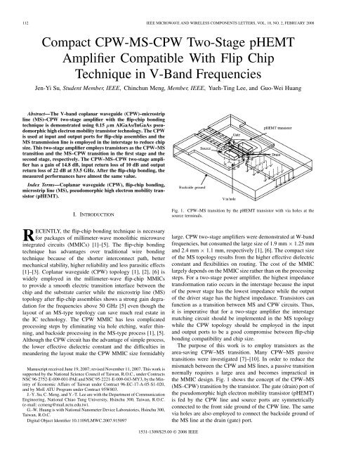
Fig. 1. <strong>CPW</strong>–<strong>MS</strong> transition by the <strong>pHEMT</strong> transistor with via holes at the<br />
source terminals.<br />
large. <strong>CPW</strong> two-stage amplifiers were demonstrated at W-band<br />
frequencies, but consumed the large size of 1.9 mm 1.25 mm<br />
and 2.4 mm 1.1 mm, respectively [1], [6]. The compact size<br />
of the <strong>MS</strong> topology results from the higher effective dielectric<br />
constant and flexibilities on routing. The cost of the MMIC<br />
largely depends on the MMIC size rather than on the processing<br />
steps. For a two-stage power amplifier, the highest impedance<br />
transformation ratio occurs in the interstage because the input<br />
of the power stage has the lowest impedance while the output<br />
of the driver stage has the highest impedance. Transistors can<br />
function as a transition between <strong>MS</strong> and <strong>CPW</strong> circuits. Thus,<br />
it is imperative that for a two-stage amplifier the interstage<br />
matching circuit should be implemented in the <strong>MS</strong> topology<br />
while the <strong>CPW</strong> topology should be employed in the input<br />
and output ports to be a good compromise between flip-chip<br />
bonding compatibility and chip size.<br />
The purpose of this work is to employ transistors as the<br />
area-saving <strong>CPW</strong>–<strong>MS</strong> transition. Many <strong>CPW</strong>–<strong>MS</strong> passive<br />
transitions were investigated [7]–[10]. In order to reduce the<br />
mismatch between the <strong>CPW</strong> and <strong>MS</strong> lines, a passive transition<br />
normally requires a large area and becomes impractical in<br />
the MMIC design. Fig. 1 shows the concept of the <strong>CPW</strong>–<strong>MS</strong><br />
(<strong>MS</strong>–<strong>CPW</strong>) transition by the transistor. The gate (drain) port of<br />
the pseudomorphic high electron mobility transistor (<strong>pHEMT</strong>)<br />
is fed by the <strong>CPW</strong> line and source ports are symmetrically<br />
connected to the front side ground of the <strong>CPW</strong> line. The same<br />
via holes are also employed to connect the backside ground of<br />
the <strong>MS</strong> line at the drain (gate) port.<br />
1531-1309/$25.00 © 2008 <strong>IEEE</strong>
SU et al.: COMPACT <strong>CPW</strong>-<strong>MS</strong>-<strong>CPW</strong> TWO-STAGE PHEMT AMPLIFIER 113<br />
Fig. 3. V-band <strong>CPW</strong>–<strong>MS</strong>–<strong>CPW</strong> two-stage <strong>pHEMT</strong> amplifier.<br />
Fig. 2. Gain curves of the <strong>MS</strong>–<strong>MS</strong>, <strong>CPW</strong>–<strong>MS</strong>, <strong>MS</strong>–<strong>CPW</strong>, and <strong>CPW</strong>–<strong>CPW</strong><br />
one-stage amplifiers with the same impedance matching.<br />
<strong>MS</strong>–<strong>MS</strong>, <strong>MS</strong>–<strong>CPW</strong>, <strong>CPW</strong>–<strong>MS</strong>, and <strong>CPW</strong>–<strong>CPW</strong> one-stage<br />
<strong>pHEMT</strong> amplifiers designed at 60 GHz are employed to study<br />
the effect of using the device as a transition. Fig. 2 shows the<br />
simulation results for these four designs. All of the four designs<br />
have the same impedance matching as shown in Fig. 2. The<br />
input/output return loss is better than 10 dB for frequencies<br />
from 58.5 to 61.5 GHz for these four designs. Thus, the effect of<br />
loss is more pronounced at the resonant matching frequencies<br />
as shown in Fig. 2. It is well known that a <strong>CPW</strong> transmission<br />
line suffers more metal loss because the electric field is more<br />
concentrated at the metal edge in a <strong>CPW</strong> transmission line.<br />
Thus, the <strong>MS</strong>–<strong>MS</strong> one-stage amplifier has the highest peak<br />
gain of 9.4 dB while the <strong>CPW</strong>–<strong>CPW</strong> one-stage amplifier has<br />
the lowest peak gain of 8.0 dB. The metal loss causes 1.4 dB<br />
peak gain degradation for the <strong>CPW</strong>–<strong>CPW</strong> configuration and<br />
0.7 dB for both <strong>CPW</strong>–<strong>MS</strong>/<strong>MS</strong>–<strong>CPW</strong> configurations when the<br />
<strong>MS</strong>–<strong>MS</strong> one-stage amplifier is compared. The loss occurring<br />
mostly at the resonant matching frequency band also affects the<br />
bandwidth. The 3 dB gain bandwidth is 7.7, 8.4, and 9.2 GHz<br />
for <strong>MS</strong>–<strong>MS</strong>, <strong>MS</strong>–<strong>CPW</strong>/<strong>CPW</strong>–<strong>MS</strong> and <strong>CPW</strong>–<strong>CPW</strong> configurations,<br />
respectively. Consequently, the <strong>CPW</strong>–<strong>MS</strong>–<strong>CPW</strong><br />
two-stage amplifier is a good topology for V-band flip-chip<br />
amplifiers in terms of gain, bandwidth, and chip size. In this<br />
work, a <strong>CPW</strong>–<strong>MS</strong>–<strong>CPW</strong> two-stage amplifier is demonstrated<br />
at V-band frequencies and the resulting amplifier shows no<br />
electric performance degradation after flip-chip mounting.<br />
II. CIRCUIT DESIGN<br />
The schematic of the <strong>CPW</strong>–<strong>MS</strong>–<strong>CPW</strong> two-stage amplifier is<br />
shown in Fig. 3 and the die photo is shown in Fig. 4. The size of<br />
the chip is 1.75 0.85 mm . This size is much smaller than the<br />
chip sizes of published [1], [6]. parameters for both the passive<br />
elements and transistors are needed in the amplifier design. The<br />
parameters of the passive elements are obtained through the<br />
EM simulator for better accuracy while the measured parameters<br />
of the <strong>pHEMT</strong> transistors are used. The <strong>CPW</strong>–<strong>MS</strong>–<strong>CPW</strong><br />
two-stage amplifier is designed for the maximum gain because<br />
Fig. 4. Die photo of the <strong>CPW</strong>–<strong>MS</strong>–<strong>CPW</strong> two-stage <strong>pHEMT</strong> amplifier.<br />
the devices are unconditionally stable at 50 GHz when the voltages<br />
of and are 2.0 V and 0 V, respectively. The width<br />
of two <strong>pHEMT</strong> transistors in the amplifier is 2 50 m. In<br />
Fig. 3, several the – series elements and elements at drain<br />
and gate ports are designed to avoid the low-frequency oscillation<br />
and to enhance the out-band stability, respectively [6]. As<br />
shown in Fig. 4, the quarter-wavelength transmission lines with<br />
a characteristic impedance of 90 are applied to the biasing networks<br />
at gate and drain terminals of the transistors. This transmission<br />
line design aims to isolate the RF signal through dc<br />
paths. The matching networks at both input and output of the<br />
two-stage amplifier are designed and realized using <strong>CPW</strong>-type<br />
transmission lines for flip-chip assembly. Additionally, the microstrip<br />
transmission line, which has a higher effective dielectric<br />
constant than <strong>CPW</strong> line has, is applied to realize the matching<br />
network between two transistors for miniaturizing the size of<br />
the amplifier.<br />
III. FLIP-CHIP MEASUREMENT RESULTS<br />
The -parameter was measured from 2 to 110 GHz by HP<br />
Network Analyzer 8510XF. Fig. 5 shows a flip-chip micrograph<br />
of the V-band <strong>CPW</strong>-<strong>MS</strong>-<strong>CPW</strong> two-stage amplifier. The substrate<br />
carrier is made of alumina. The carrier has the feedline<br />
patterns including dc bias lines and 50 <strong>CPW</strong> transmission<br />
lines in Fig. 5. The feedline patterns and chip pads are connected<br />
by the flip-chip bonding bumps. The flip-chip bonding<br />
bump sizes are 50 m in diameter and 30 m in height.<br />
As shown in Fig. 6(a) and (b), the measured -parameters<br />
of the V-band two-stage amplifier with and without flip-chip<br />
bonding are very similar. The peak of the amplifier without<br />
flip-chip bonding is 14.81 dB at 53.5 GHz. After using the<br />
flip-chip bonding technique, the amplitude and frequency of the<br />
peak are slightly reduced and shifted to 14.52 and 53 GHz,<br />
respectively. The with and without flip-chip bonding are
114 <strong>IEEE</strong> MICROWAVE AND WIRELESS COMPONENTS LETTERS, VOL. 18, NO. 2, FEBRUARY 2008<br />
Fig. 5. Flip-chip photograph of the <strong>CPW</strong>–<strong>MS</strong>–<strong>CPW</strong> two-stage <strong>pHEMT</strong> amplifier.<br />
13.3 dB and 18.1 dB near the operating frequency of<br />
55 GHz, and the of them are lower than 30 dB anywhere.<br />
Obviously, the reverse isolation of the flip-chip technique<br />
is insignificant to the performance of the bare-chip. of<br />
two curves are almost kept the same. The deepest without<br />
flip-chip bonding is 27 dB at 53.5 GHz, and the lowest<br />
with flip-chip bonding is 23 dB at 53.0 GHz. The measured<br />
results show the feasibilities of this design approach utilizing<br />
the <strong>CPW</strong>–<strong>MS</strong>–<strong>CPW</strong> topology for flip-chip bonding techniques.<br />
Besides, the simulation results and measured results without<br />
flip-chip bonding are also shown in Fig. 6(a) and (b) for comparison.<br />
The simulation results agree well with the measured<br />
results. Thus, the <strong>CPW</strong>–<strong>MS</strong>/<strong>MS</strong>–<strong>CPW</strong> transitions by the transistor<br />
device are wideband in nature.<br />
IV. CONCLUSION<br />
The V-band <strong>CPW</strong>-<strong>MS</strong>-<strong>CPW</strong> two-stage amplifier compatible<br />
with flip-chip bonding techniques is proposed and<br />
demonstrated. The input and output networks of the proposed<br />
amplifier are constructed by the <strong>CPW</strong>-based transmission lines,<br />
forming the smooth electric interfaces for the flip-chip bonding<br />
package. Additionally, the proposed compact <strong>CPW</strong>-<strong>MS</strong>-<strong>CPW</strong><br />
transition, which effectively integrates the <strong>pHEMT</strong> transistors,<br />
successfully converts the electromagnetic energy from the<br />
<strong>CPW</strong> mode to the <strong>MS</strong> mode. Such that the transition provides<br />
a wide degree of freedom to design the <strong>pHEMT</strong> amplifier with<br />
both <strong>CPW</strong> and microstrip elements. The prototype is fabricated<br />
using AlGaAs/InGaAs 0.15 m <strong>pHEMT</strong> technology.<br />
After the prototype is packaged through the flip-chip bonding<br />
technology, there is negligible change on the electric characteristics.<br />
The measured results demonstrate the feasibility of the<br />
proposed <strong>CPW</strong>-<strong>MS</strong>-<strong>CPW</strong> two-stage <strong>pHEMT</strong> amplifier design<br />
for flip-chip bonding techniques.<br />
REFERENCES<br />
[1] T. Hirose, K. Makiyama, K. Ono, T. M. Shimura, S. Aoki, Y. Ohashi, S.<br />
Yokokawa, and Y. Watanabe, “A flip-chip MMIC design with coplanar<br />
waveguide transmission line in the W-Band,” <strong>IEEE</strong> Trans. Microw.<br />
Theory Tech., vol. 46, no. 12, pp. 2276–2282, Dec. 1998.<br />
[2] A. Tessmann, M. Riessle, S. Kudszus, and H. Massler, “A flip-chip<br />
packaged coplanar 94 GHz amplifier module with efficient suppression<br />
of parasitic substrate effects,” <strong>IEEE</strong> Microw. Wireless Compon. Lett.,<br />
vol. 14, no. 4, pp. 145–147, Apr. 2004.<br />
[3] Y. Arai, M. Sato, H. T. Yamada, T. Hamada, K. Nagai, and H. I. Fujishiro,<br />
“60-GHz flip-chip assembled MIC design considering chipsubstrate<br />
effect,” <strong>IEEE</strong> Trans. Microw. Theory Tech., vol. 45, no. 12,<br />
pp. 2261–2266, Dec. 1997.<br />
(b)<br />
Fig. 6. (a) S and S and (b) S and S of the simulated (without flip-chip<br />
bonding) and measured (with and without flip-chip bonding) <strong>CPW</strong>–<strong>MS</strong>–<strong>CPW</strong><br />
two-stage <strong>pHEMT</strong> amplifier.<br />
[4] A. Jentzsch and W. Heinrich, “Theory and measurement of flip-chip<br />
interconnects for frequencies up to 100 GHz,” <strong>IEEE</strong> Trans. Microw.<br />
Theory Tech, vol. 49, no. 5, pp. 871–878, May 2001.<br />
[5] C. Kärnfelt, H. Zirath, J. P. Starski, and J. Rudnicki, “Flip chip assembly<br />
of a 40–60 GHz GaAs microstrip amplifier,” in Proc. 34th Eur.<br />
Microw. Conf., Amsterdam, The Netherlands, Oct. 11–15, 2004, vol.<br />
1, pp. 89–92.<br />
[6] M. Yu, M. Matloubian, P. Petre, L. R. Hamilton, R. Bowen, M. Lui,<br />
H.-C. Sun, C. M. Ngo, P. Janke, D. W. Baker, and R. S. Robertson,<br />
“W-band InP HEMT MMIC’s using finite-ground coplanar waveguide<br />
(FG<strong>CPW</strong>) design,” <strong>IEEE</strong> J. Solid-State Circuits, vol. 34, no. 9, pp.<br />
1212–1218, Sep. 1999.<br />
[7] G. P. Gauthier, L. P. Katehi, and G. M. Rebeiz, “W-Band finite ground<br />
coplanar waveguide (FG<strong>CPW</strong>) to microstrip line transition,” in <strong>IEEE</strong><br />
MTT-S Int. Dig., 1998, pp. 107–109.<br />
[8] W. Heinrich, A. Jentzsch, and G. Baumann, “Millimeter-wave characteristics<br />
of flip-chip interconnects for multichip modules,” <strong>IEEE</strong> Trans.<br />
Microw. Theory Tech, vol. 46, no. 12, pp. 2264–2268, Dec. 1998.<br />
[9] L. Zhu and W. Menzel, “Broad-band microstrip-to-<strong>CPW</strong> transition via<br />
frequency-dependent electromagnetic coupling,” <strong>IEEE</strong> Trans. Microw.<br />
Theory Tech, vol. 52, no. 5, pp. 1517–1522, May 2004.<br />
[10] A. M. E. Safwat, K. A. Zaki, W. Johnson, and C. H. Lee, “Novel transition<br />
between different configurations of planar transmission lines,”<br />
<strong>IEEE</strong> Microw. Wireless Compon. Lett., vol. 12, no. 4, pp. 128–130,<br />
Apr. 2002.