Compact CPW-MS-CPW Two-Stage pHEMT Amplifier ... - IEEE Xplore
Compact CPW-MS-CPW Two-Stage pHEMT Amplifier ... - IEEE Xplore
Compact CPW-MS-CPW Two-Stage pHEMT Amplifier ... - IEEE Xplore

Create successful ePaper yourself
Turn your PDF publications into a flip-book with our unique Google optimized e-Paper software.
SU et al.: COMPACT <strong>CPW</strong>-<strong>MS</strong>-<strong>CPW</strong> TWO-STAGE PHEMT AMPLIFIER 113<br />
Fig. 3. V-band <strong>CPW</strong>–<strong>MS</strong>–<strong>CPW</strong> two-stage <strong>pHEMT</strong> amplifier.<br />
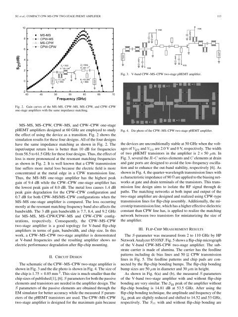
Fig. 2. Gain curves of the <strong>MS</strong>–<strong>MS</strong>, <strong>CPW</strong>–<strong>MS</strong>, <strong>MS</strong>–<strong>CPW</strong>, and <strong>CPW</strong>–<strong>CPW</strong><br />
one-stage amplifiers with the same impedance matching.<br />
<strong>MS</strong>–<strong>MS</strong>, <strong>MS</strong>–<strong>CPW</strong>, <strong>CPW</strong>–<strong>MS</strong>, and <strong>CPW</strong>–<strong>CPW</strong> one-stage<br />
<strong>pHEMT</strong> amplifiers designed at 60 GHz are employed to study<br />
the effect of using the device as a transition. Fig. 2 shows the<br />
simulation results for these four designs. All of the four designs<br />
have the same impedance matching as shown in Fig. 2. The<br />
input/output return loss is better than 10 dB for frequencies<br />
from 58.5 to 61.5 GHz for these four designs. Thus, the effect of<br />
loss is more pronounced at the resonant matching frequencies<br />
as shown in Fig. 2. It is well known that a <strong>CPW</strong> transmission<br />
line suffers more metal loss because the electric field is more<br />
concentrated at the metal edge in a <strong>CPW</strong> transmission line.<br />
Thus, the <strong>MS</strong>–<strong>MS</strong> one-stage amplifier has the highest peak<br />
gain of 9.4 dB while the <strong>CPW</strong>–<strong>CPW</strong> one-stage amplifier has<br />
the lowest peak gain of 8.0 dB. The metal loss causes 1.4 dB<br />
peak gain degradation for the <strong>CPW</strong>–<strong>CPW</strong> configuration and<br />
0.7 dB for both <strong>CPW</strong>–<strong>MS</strong>/<strong>MS</strong>–<strong>CPW</strong> configurations when the<br />
<strong>MS</strong>–<strong>MS</strong> one-stage amplifier is compared. The loss occurring<br />
mostly at the resonant matching frequency band also affects the<br />
bandwidth. The 3 dB gain bandwidth is 7.7, 8.4, and 9.2 GHz<br />
for <strong>MS</strong>–<strong>MS</strong>, <strong>MS</strong>–<strong>CPW</strong>/<strong>CPW</strong>–<strong>MS</strong> and <strong>CPW</strong>–<strong>CPW</strong> configurations,<br />
respectively. Consequently, the <strong>CPW</strong>–<strong>MS</strong>–<strong>CPW</strong><br />
two-stage amplifier is a good topology for V-band flip-chip<br />
amplifiers in terms of gain, bandwidth, and chip size. In this<br />
work, a <strong>CPW</strong>–<strong>MS</strong>–<strong>CPW</strong> two-stage amplifier is demonstrated<br />
at V-band frequencies and the resulting amplifier shows no<br />
electric performance degradation after flip-chip mounting.<br />
II. CIRCUIT DESIGN<br />
The schematic of the <strong>CPW</strong>–<strong>MS</strong>–<strong>CPW</strong> two-stage amplifier is<br />
shown in Fig. 3 and the die photo is shown in Fig. 4. The size of<br />
the chip is 1.75 0.85 mm . This size is much smaller than the<br />
chip sizes of published [1], [6]. parameters for both the passive<br />
elements and transistors are needed in the amplifier design. The<br />
parameters of the passive elements are obtained through the<br />
EM simulator for better accuracy while the measured parameters<br />
of the <strong>pHEMT</strong> transistors are used. The <strong>CPW</strong>–<strong>MS</strong>–<strong>CPW</strong><br />
two-stage amplifier is designed for the maximum gain because<br />
Fig. 4. Die photo of the <strong>CPW</strong>–<strong>MS</strong>–<strong>CPW</strong> two-stage <strong>pHEMT</strong> amplifier.<br />
the devices are unconditionally stable at 50 GHz when the voltages<br />
of and are 2.0 V and 0 V, respectively. The width<br />
of two <strong>pHEMT</strong> transistors in the amplifier is 2 50 m. In<br />
Fig. 3, several the – series elements and elements at drain<br />
and gate ports are designed to avoid the low-frequency oscillation<br />
and to enhance the out-band stability, respectively [6]. As<br />
shown in Fig. 4, the quarter-wavelength transmission lines with<br />
a characteristic impedance of 90 are applied to the biasing networks<br />
at gate and drain terminals of the transistors. This transmission<br />
line design aims to isolate the RF signal through dc<br />
paths. The matching networks at both input and output of the<br />
two-stage amplifier are designed and realized using <strong>CPW</strong>-type<br />
transmission lines for flip-chip assembly. Additionally, the microstrip<br />
transmission line, which has a higher effective dielectric<br />
constant than <strong>CPW</strong> line has, is applied to realize the matching<br />
network between two transistors for miniaturizing the size of<br />
the amplifier.<br />
III. FLIP-CHIP MEASUREMENT RESULTS<br />
The -parameter was measured from 2 to 110 GHz by HP<br />
Network Analyzer 8510XF. Fig. 5 shows a flip-chip micrograph<br />
of the V-band <strong>CPW</strong>-<strong>MS</strong>-<strong>CPW</strong> two-stage amplifier. The substrate<br />
carrier is made of alumina. The carrier has the feedline<br />
patterns including dc bias lines and 50 <strong>CPW</strong> transmission<br />
lines in Fig. 5. The feedline patterns and chip pads are connected<br />
by the flip-chip bonding bumps. The flip-chip bonding<br />
bump sizes are 50 m in diameter and 30 m in height.<br />
As shown in Fig. 6(a) and (b), the measured -parameters<br />
of the V-band two-stage amplifier with and without flip-chip<br />
bonding are very similar. The peak of the amplifier without<br />
flip-chip bonding is 14.81 dB at 53.5 GHz. After using the<br />
flip-chip bonding technique, the amplitude and frequency of the<br />
peak are slightly reduced and shifted to 14.52 and 53 GHz,<br />
respectively. The with and without flip-chip bonding are