Compact CPW-MS-CPW Two-Stage pHEMT Amplifier ... - IEEE Xplore
Compact CPW-MS-CPW Two-Stage pHEMT Amplifier ... - IEEE Xplore
Compact CPW-MS-CPW Two-Stage pHEMT Amplifier ... - IEEE Xplore

You also want an ePaper? Increase the reach of your titles
YUMPU automatically turns print PDFs into web optimized ePapers that Google loves.
114 <strong>IEEE</strong> MICROWAVE AND WIRELESS COMPONENTS LETTERS, VOL. 18, NO. 2, FEBRUARY 2008<br />
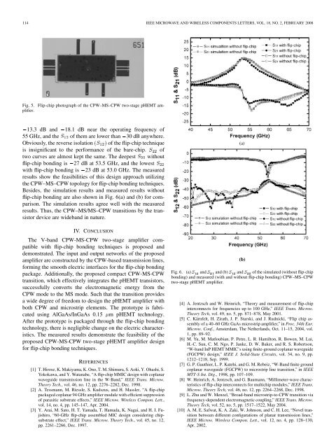
Fig. 5. Flip-chip photograph of the <strong>CPW</strong>–<strong>MS</strong>–<strong>CPW</strong> two-stage <strong>pHEMT</strong> amplifier.<br />
13.3 dB and 18.1 dB near the operating frequency of<br />
55 GHz, and the of them are lower than 30 dB anywhere.<br />
Obviously, the reverse isolation of the flip-chip technique<br />
is insignificant to the performance of the bare-chip. of<br />
two curves are almost kept the same. The deepest without<br />
flip-chip bonding is 27 dB at 53.5 GHz, and the lowest<br />
with flip-chip bonding is 23 dB at 53.0 GHz. The measured<br />
results show the feasibilities of this design approach utilizing<br />
the <strong>CPW</strong>–<strong>MS</strong>–<strong>CPW</strong> topology for flip-chip bonding techniques.<br />
Besides, the simulation results and measured results without<br />
flip-chip bonding are also shown in Fig. 6(a) and (b) for comparison.<br />
The simulation results agree well with the measured<br />
results. Thus, the <strong>CPW</strong>–<strong>MS</strong>/<strong>MS</strong>–<strong>CPW</strong> transitions by the transistor<br />
device are wideband in nature.<br />
IV. CONCLUSION<br />
The V-band <strong>CPW</strong>-<strong>MS</strong>-<strong>CPW</strong> two-stage amplifier compatible<br />
with flip-chip bonding techniques is proposed and<br />
demonstrated. The input and output networks of the proposed<br />
amplifier are constructed by the <strong>CPW</strong>-based transmission lines,<br />
forming the smooth electric interfaces for the flip-chip bonding<br />
package. Additionally, the proposed compact <strong>CPW</strong>-<strong>MS</strong>-<strong>CPW</strong><br />
transition, which effectively integrates the <strong>pHEMT</strong> transistors,<br />
successfully converts the electromagnetic energy from the<br />
<strong>CPW</strong> mode to the <strong>MS</strong> mode. Such that the transition provides<br />
a wide degree of freedom to design the <strong>pHEMT</strong> amplifier with<br />
both <strong>CPW</strong> and microstrip elements. The prototype is fabricated<br />
using AlGaAs/InGaAs 0.15 m <strong>pHEMT</strong> technology.<br />
After the prototype is packaged through the flip-chip bonding<br />
technology, there is negligible change on the electric characteristics.<br />
The measured results demonstrate the feasibility of the<br />
proposed <strong>CPW</strong>-<strong>MS</strong>-<strong>CPW</strong> two-stage <strong>pHEMT</strong> amplifier design<br />
for flip-chip bonding techniques.<br />
REFERENCES<br />
[1] T. Hirose, K. Makiyama, K. Ono, T. M. Shimura, S. Aoki, Y. Ohashi, S.<br />
Yokokawa, and Y. Watanabe, “A flip-chip MMIC design with coplanar<br />
waveguide transmission line in the W-Band,” <strong>IEEE</strong> Trans. Microw.<br />
Theory Tech., vol. 46, no. 12, pp. 2276–2282, Dec. 1998.<br />
[2] A. Tessmann, M. Riessle, S. Kudszus, and H. Massler, “A flip-chip<br />
packaged coplanar 94 GHz amplifier module with efficient suppression<br />
of parasitic substrate effects,” <strong>IEEE</strong> Microw. Wireless Compon. Lett.,<br />
vol. 14, no. 4, pp. 145–147, Apr. 2004.<br />
[3] Y. Arai, M. Sato, H. T. Yamada, T. Hamada, K. Nagai, and H. I. Fujishiro,<br />
“60-GHz flip-chip assembled MIC design considering chipsubstrate<br />
effect,” <strong>IEEE</strong> Trans. Microw. Theory Tech., vol. 45, no. 12,<br />
pp. 2261–2266, Dec. 1997.<br />
(b)<br />
Fig. 6. (a) S and S and (b) S and S of the simulated (without flip-chip<br />
bonding) and measured (with and without flip-chip bonding) <strong>CPW</strong>–<strong>MS</strong>–<strong>CPW</strong><br />
two-stage <strong>pHEMT</strong> amplifier.<br />
[4] A. Jentzsch and W. Heinrich, “Theory and measurement of flip-chip<br />
interconnects for frequencies up to 100 GHz,” <strong>IEEE</strong> Trans. Microw.<br />
Theory Tech, vol. 49, no. 5, pp. 871–878, May 2001.<br />
[5] C. Kärnfelt, H. Zirath, J. P. Starski, and J. Rudnicki, “Flip chip assembly<br />
of a 40–60 GHz GaAs microstrip amplifier,” in Proc. 34th Eur.<br />
Microw. Conf., Amsterdam, The Netherlands, Oct. 11–15, 2004, vol.<br />
1, pp. 89–92.<br />
[6] M. Yu, M. Matloubian, P. Petre, L. R. Hamilton, R. Bowen, M. Lui,<br />
H.-C. Sun, C. M. Ngo, P. Janke, D. W. Baker, and R. S. Robertson,<br />
“W-band InP HEMT MMIC’s using finite-ground coplanar waveguide<br />
(FG<strong>CPW</strong>) design,” <strong>IEEE</strong> J. Solid-State Circuits, vol. 34, no. 9, pp.<br />
1212–1218, Sep. 1999.<br />
[7] G. P. Gauthier, L. P. Katehi, and G. M. Rebeiz, “W-Band finite ground<br />
coplanar waveguide (FG<strong>CPW</strong>) to microstrip line transition,” in <strong>IEEE</strong><br />
MTT-S Int. Dig., 1998, pp. 107–109.<br />
[8] W. Heinrich, A. Jentzsch, and G. Baumann, “Millimeter-wave characteristics<br />
of flip-chip interconnects for multichip modules,” <strong>IEEE</strong> Trans.<br />
Microw. Theory Tech, vol. 46, no. 12, pp. 2264–2268, Dec. 1998.<br />
[9] L. Zhu and W. Menzel, “Broad-band microstrip-to-<strong>CPW</strong> transition via<br />
frequency-dependent electromagnetic coupling,” <strong>IEEE</strong> Trans. Microw.<br />
Theory Tech, vol. 52, no. 5, pp. 1517–1522, May 2004.<br />
[10] A. M. E. Safwat, K. A. Zaki, W. Johnson, and C. H. Lee, “Novel transition<br />
between different configurations of planar transmission lines,”<br />
<strong>IEEE</strong> Microw. Wireless Compon. Lett., vol. 12, no. 4, pp. 128–130,<br />
Apr. 2002.