Design Methodologies of LTCC Bandpass Filters, Diplexer, and ...
Design Methodologies of LTCC Bandpass Filters, Diplexer, and ...
Design Methodologies of LTCC Bandpass Filters, Diplexer, and ...

You also want an ePaper? Increase the reach of your titles
YUMPU automatically turns print PDFs into web optimized ePapers that Google loves.
IEEE TRANSACTIONS ON MICROWAVE THEORY AND TECHNIQUES, VOL. 54, NO. 2, FEBRUARY 2006 717<br />
<strong>Design</strong> <strong>Methodologies</strong> <strong>of</strong> <strong>LTCC</strong> <strong>B<strong>and</strong>pass</strong> <strong>Filters</strong>,<br />
<strong>Diplexer</strong>, <strong>and</strong> Triplexer With Transmission Zeros<br />
Ching-Wen Tang, Member, IEEE, <strong>and</strong> Sheng-Fu You<br />
Abstract—A new method for designing the multilayered filter,<br />
diplexer, <strong>and</strong> triplexer is proposed in this paper. The main structure<br />
<strong>of</strong> the multilayered filter is a parallel-coupled line connected<br />
with a capacitor. By properly controlling the coupling coefficient<br />
between the parallel-coupled line <strong>and</strong> the capacitor, the transmission<br />
zero will appear at the lower or higher passb<strong>and</strong>’s skirt. Moreover,<br />
such characteristics can be employed to design the diplexer as<br />
well for dual- or quad-b<strong>and</strong> portable telephones. In order to miniaturize<br />
the size <strong>of</strong> the circuit <strong>and</strong> to improve its performance, multilayered<br />
structure <strong>and</strong> the low-temperature co-fired ceramic technology<br />
are employed to design <strong>and</strong> fabricate the filter. Theoretical<br />
analysis <strong>and</strong> design procedures are also provided. Measurement results<br />
<strong>of</strong> fabricated examples are shown to match well with the electromagnetic<br />
simulation, which validate the proposed structure.<br />
Index Terms—<strong>B<strong>and</strong>pass</strong> filter, diplexer, low-temperature c<strong>of</strong>ired<br />
ceramic (<strong>LTCC</strong>).<br />
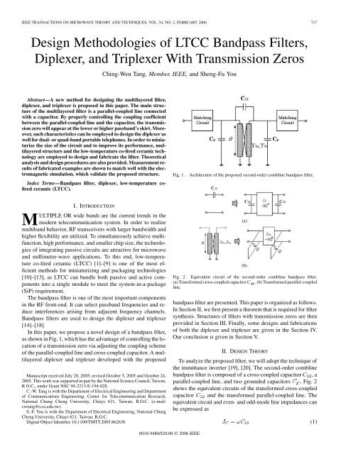
Fig. 1.<br />
Architecture <strong>of</strong> the proposed second-order combline b<strong>and</strong>pass filter.<br />
I. INTRODUCTION<br />
MULTIPLE OR wide b<strong>and</strong>s are the current trends in the<br />
modern telecommunication system. In order to realize<br />
multib<strong>and</strong> behavior, RF transceivers with larger b<strong>and</strong>width <strong>and</strong><br />
higher flexibility are utilized. To simultaneously achieve multifunction,<br />
high performance, <strong>and</strong> smaller chip size, the technologies<br />
<strong>of</strong> integrating passive circuits are attractive for microwave<br />
<strong>and</strong> millimeter-wave applications. To this end, low-temperature<br />
co-fired ceramic (<strong>LTCC</strong>) [1]–[9] is one <strong>of</strong> the most efficient<br />
methods for miniaturizing <strong>and</strong> packaging technologies<br />
[10]–[13], as <strong>LTCC</strong> can bundle both passive <strong>and</strong> active components<br />
into a single module to meet the system-in-a-package<br />
(SiP) requirement.<br />
The b<strong>and</strong>pass filter is one <strong>of</strong> the most important components<br />
in the RF front-end. It can select passb<strong>and</strong> frequencies <strong>and</strong> reduce<br />
interferences arising from adjacent frequency channels.<br />
<strong>B<strong>and</strong>pass</strong> filters are used to design the diplexer <strong>and</strong> triplexer<br />
[14]–[18].<br />
In this paper, we propose a novel design <strong>of</strong> a b<strong>and</strong>pass filter,<br />
as shown in Fig. 1, which has the advantage <strong>of</strong> controlling the location<br />
<strong>of</strong> a transmission zero via adjusting the coupling scheme<br />
<strong>of</strong> the parallel-coupled line <strong>and</strong> cross-coupled capacitor. A multilayered<br />
diplexer <strong>and</strong> triplexer developed with the proposed<br />
Manuscript received July 20, 2005; revised October 5, 2005 <strong>and</strong> October 24,<br />
2005. This work was supported in part by the National Science Council, Taiwan,<br />
R.O.C., under Grant NSC 94-2213-E-194-028.<br />
C.-W. Tang is with the Department <strong>of</strong> Electrical Engineering <strong>and</strong> Department<br />
<strong>of</strong> Communications Engineering, Center for Telecommunication Research,<br />
National Chung Cheng University, Chiayi 621, Taiwan, R.O.C. (e-mail:<br />
cwtang@ccu.edu.tw).<br />
S.-F. You is with the Department <strong>of</strong> Electrical Engineering, National Chung<br />
Cheng University, Chiayi 621, Taiwan, R.O.C.<br />
Digital Object Identifier 10.1109/TMTT.2005.862638<br />
Fig. 2. Equivalent circuit <strong>of</strong> the second-order combline b<strong>and</strong>pass filter.<br />
(a) Transformed cross-coupled capacitor C . (b) Transformed parallel-coupled<br />
line.<br />
b<strong>and</strong>pass filter are presented. This paper is organized as follows.<br />
In Section II, we first present a theorem that is required for filter<br />
synthesis. Structures <strong>of</strong> filters with transmission zeros are then<br />
provided in Section III. Finally, some designs <strong>and</strong> fabrications<br />
<strong>of</strong> both the diplexer <strong>and</strong> triplexer are given in the Section IV.<br />
Our conclusion is given in Section V.<br />
II. DESIGN THEORY<br />
To analyze the proposed filter, we will adopt the technique <strong>of</strong><br />
the immittance inverter [19], [20]. The second-order combline<br />
b<strong>and</strong>pass filter is composed <strong>of</strong> a cross-coupled capacitor ,a<br />
parallel-coupled line, <strong>and</strong> two grounded capacitors . Fig. 2<br />
shows the equivalent circuits <strong>of</strong> the transformed cross-coupled<br />
capacitor <strong>and</strong> the transformed parallel-coupled line. The<br />
equivalent circuit <strong>and</strong> even- <strong>and</strong> odd-mode line impedances can<br />
be expressed as<br />
(1)<br />
0018-9480/$20.00 © 2006 IEEE
718 IEEE TRANSACTIONS ON MICROWAVE THEORY AND TECHNIQUES, VOL. 54, NO. 2, FEBRUARY 2006<br />
Fig. 3.<br />
filter.<br />
Equivalent circuit <strong>of</strong> the proposed second-order combline b<strong>and</strong>pass<br />
Fig. 5. Transformations for the matching circuit in the source <strong>and</strong> load ports.<br />
(a) Positive J-inverter. (b) Negative J-inverter.<br />
is resonance at the central frequency, which will result<br />
in . The capacitor can be derived as<br />
Fig. 4.<br />
Equivalent circuit <strong>of</strong> the generalized b<strong>and</strong>pass filter.<br />
where <strong>and</strong> are, respectively, the odd- <strong>and</strong> even-mode<br />
admittances <strong>of</strong> coupled transmission line, <strong>and</strong> is the corresponding<br />
electric length.<br />
Adding two circuits shown in Fig. 2, <strong>and</strong> shunting with two<br />
grounded capacitors at two ports separately yields the complete<br />
equivalent circuit <strong>of</strong> the b<strong>and</strong>pass filter, as shown in Fig. 3.<br />
Thus, we can apply the immittance inverter to analyze <strong>and</strong> design<br />
b<strong>and</strong>pass filters. The admittance inverter <strong>and</strong> capacitor<br />
are derived as<br />
Following the equivalent circuit in Fig. 3, the equivalent circuit<br />
<strong>of</strong> the generalized b<strong>and</strong>pass filter can also be expressed as<br />
Fig. 4, which includes the admittance inverter. The admittance<br />
inverters, susceptance, <strong>and</strong> its slope parameter are, respectively,<br />
given by<br />
(2)<br />
(3)<br />
(4)<br />
(5)<br />
(6)<br />
(7)<br />
(8)<br />
(9)<br />
(10)<br />
where the ’s are the element values <strong>of</strong> the prototype lowpass<br />
filter, is the fractional b<strong>and</strong>width, <strong>and</strong> <strong>and</strong> are<br />
the impedances <strong>of</strong> source <strong>and</strong> load transmission lines, respectively<br />
[19].<br />
(11)<br />
where <strong>and</strong> are electrical length <strong>and</strong> angular frequency at<br />
the central frequency, respectively.<br />
The b<strong>and</strong>pass filter with a transmission zero located at the<br />
angular frequency will make . at the center<br />
frequency <strong>and</strong> can be derived as<br />
when<br />
when<br />
(12)<br />
(13)<br />
The matching circuits located at source <strong>and</strong> load ports,<br />
as shown in Fig. 1, can be implemented using the following<br />
methods. Note that the quarter-wavelength transmission line is<br />
the simplest form <strong>of</strong> inverters <strong>and</strong>, on the other h<strong>and</strong>, the inductance<br />
or capacitance -network to substitute the -inverter<br />
is the other method. Since the negative inductance or capacitance<br />
cannot be employed to the source or load impedance, a<br />
transformation is needed, as shown in Fig. 5. These equations<br />
are revealed as<br />
III. FILTER DESIGN WITH TRANSMISSION ZERO<br />
(14)<br />
(15)<br />
(16)<br />
(17)<br />
Here, two examples are presented to explain the location <strong>of</strong><br />
the frequency <strong>of</strong> the transmission zero, which will appear at the<br />
lower or higher skirt <strong>of</strong> the passb<strong>and</strong>.
TANG AND YOU: DESIGN METHODOLOGIES OF <strong>LTCC</strong> BANDPASS FILTERS, DIPLEXER, AND TRIPLEXER WITH TRANSMISSION ZEROS 719<br />
Fig. 6. 2.4-GHz b<strong>and</strong>pass filter with the transmission zero at the frequency <strong>of</strong><br />
1.9 GHz. (a) Filter architecture. (b) Simulated results.<br />
A. Circuit Model<br />
The first example is a 2.4-GHz b<strong>and</strong>pass filter. Its center frequency<br />
is set at 2.4 GHz <strong>and</strong> the frequency <strong>of</strong> the transmission<br />
zero is set at 1.9 GHz. The ripple, b<strong>and</strong>width, impedance, <strong>and</strong><br />
electric length <strong>of</strong> the coupled transmission line are chosen as<br />
0.01 dB, 6%, 30 , <strong>and</strong> 12 , respectively. By making use <strong>of</strong><br />
(1)–(17) derived in Section II, one can show that the parameters<br />
<strong>of</strong> the cross-coupled capacitor , even- <strong>and</strong> odd-mode impedances<br />
<strong>and</strong> <strong>of</strong> the parallel-coupled line, <strong>and</strong> grounded capacitors<br />
are equal to 3.93 pF, 39.24 , 24.28 , <strong>and</strong> 6.47 pF,<br />
respectively. Therefore, is 0.0206. A quarter-wavelength<br />
transmission line is utilized to form the matching circuit, <strong>and</strong>,<br />
hence, the impedance <strong>of</strong> this transmission line is 48.47 , which<br />
is close to 50 , which is the vale <strong>of</strong> the system impedance.<br />
Therefore, the matching circuit can be neglected <strong>and</strong> the secondorder<br />
combline b<strong>and</strong>pass filter can be connected directly to the<br />
input <strong>and</strong> output ports, as shown in Fig. 6(a). These derived parameters<br />
<strong>and</strong> are substituted into the circuit<br />
simulator such as ADS or equivalent s<strong>of</strong>tware to carry out the<br />
circuit simulation. Simulation results <strong>of</strong> the 2.4-GHz b<strong>and</strong>pass<br />
filter are presented in Fig. 6(b).<br />
Fig. 7. 2-GHz b<strong>and</strong>pass filter with the transmission zero at the frequency <strong>of</strong><br />
2.5 GHz. (a) Filter architecture. (b) Simulated results.<br />
A 2-GHz b<strong>and</strong>pass filter is taken as the second example. Its<br />
center frequency is set at 2 GHz <strong>and</strong> the frequency <strong>of</strong> the transmission<br />
zero is set at 2.5 GHz. The ripple, b<strong>and</strong>width, impedance,<br />
<strong>and</strong> electric length <strong>of</strong> the coupled transmission line are set as 0.01<br />
dB, 7%, 30 , <strong>and</strong> 30 , respectively. The structure in Fig. 5(b)<br />
can be applied to the transformation for the matching circuit in<br />
the source <strong>and</strong> load ports. Fig. 7(a) shows the equivalent circuit<br />
<strong>of</strong> the b<strong>and</strong>pass filter with the transmission zero at the higher skirt<br />
<strong>of</strong> the passb<strong>and</strong>. Here, the parameters <strong>of</strong> the cross-coupled capacitor<br />
, even- <strong>and</strong> odd-mode impedances <strong>and</strong> <strong>of</strong> the parallel-coupled<br />
line, the grounded capacitors , <strong>and</strong> source <strong>and</strong><br />
load capacitors are calculated as 1.26 pF, 54.96 , 20.63 ,<br />
2.54 pF, <strong>and</strong> 0.8 pF, respectively. Simulation results <strong>of</strong> this 2-GHz<br />
b<strong>and</strong>pass filter are presented in Fig. 7(b).<br />
B. EM Simulation <strong>and</strong> Measurement<br />
Prior to designing the circuit, the exact parameter values <strong>of</strong><br />
ceramic sheets such as the dielectric constant <strong>and</strong> layer thickness<br />
should be known first. These values are very significant to<br />
extract physical parameters <strong>and</strong> can be critical in constructing<br />
the equivalent circuit [21].
720 IEEE TRANSACTIONS ON MICROWAVE THEORY AND TECHNIQUES, VOL. 54, NO. 2, FEBRUARY 2006<br />
Fig. 8. Fabricated 2.4-GHz b<strong>and</strong>pass filter with transmission zero at the<br />
frequency <strong>of</strong> 1.9 GHz. (a) 3-D structure. (b) Measured <strong>and</strong> EM simulated<br />
results.<br />
Two filters mentioned above are fabricated with the substrate<br />
<strong>of</strong> Dupont 951. Their dielectric constant <strong>and</strong> loss tangent are 7.8<br />
<strong>and</strong> 0.0045, respectively. The 2.4-GHz <strong>LTCC</strong> filter is designed<br />
on one upper layer with the sheet <strong>of</strong> 1.57 mil, six middle layers<br />
with the sheet <strong>of</strong> 3.6 mil, <strong>and</strong> three lower layers with the sheet<br />
<strong>of</strong> 1.57 mil. Its overall size is 110 mil 92 mil 28 mil. After<br />
circuit simulation, these values are converted into the <strong>LTCC</strong><br />
structure. The simulation is carried out with the assistant <strong>of</strong> the<br />
full-wave electromagnetic (EM) simulator Sonnet from Sonnet<br />
S<strong>of</strong>tware Inc., North Syracuse, NY. In the 3-D structure, the parallel-coupled<br />
line is placed on the lower layer to reduce the coupling<br />
effect with other capacitors. Fig. 8(a) shows the three-dimensional<br />
(3-D) structure <strong>of</strong> 2.4-GHz <strong>LTCC</strong> b<strong>and</strong>pass filter.<br />
The on-wafer tester has been chosen to improve the accuracy <strong>of</strong><br />
measurement. The network analyzer Agilent N5230A PNA_L<br />
is used to measure, <strong>and</strong> the short-open-load-through (SOLT) is<br />
adopted to calibrate.<br />
Fig. 9. Fabricated 2-GHz b<strong>and</strong>pass filter with transmission zero at the<br />
frequency <strong>of</strong> 2.5 GHz. (a) 3-D structure. (b) Measured <strong>and</strong> EM simulated<br />
results.<br />
As shown in Fig. 8(b), the frequencies <strong>of</strong> measured <strong>and</strong> EM<br />
simulated transmission zeros are 1.84 <strong>and</strong> 1.9 GHz, respectively.<br />
At the frequency <strong>of</strong> 2.4 GHz, the measured <strong>and</strong> EM simulated<br />
insertion losses are less than 1.44 <strong>and</strong> 1.3 dB, respectively; the<br />
return losses are greater than 15 <strong>and</strong> 17 dB, respectively.<br />
A 2-GHz b<strong>and</strong>pass filter is given as another design example.<br />
This 2-GHz <strong>LTCC</strong> filter is designed on five upper layers with the<br />
sheet <strong>of</strong> 3.6 mil, four middle layers with the sheet <strong>of</strong> 1.57 mil,<br />
<strong>and</strong> two lower layers with the sheet <strong>of</strong> 3.6 mil. Its overall size<br />
is 107 mil 102 mil 32 mil. The 3-D structure <strong>of</strong> the 2-GHz<br />
<strong>LTCC</strong> b<strong>and</strong>pass filter is shown in Fig. 9(a). In the 3-D structure,<br />
the parallel-coupled line is the same placed on the lower layer<br />
to reduce the coupling effect with other capacitors. As shown<br />
in Fig. 9(b), the frequencies <strong>of</strong> the measured <strong>and</strong> EM simulated<br />
transmission zeros are 2.45 <strong>and</strong> 2.5 GHz, respectively. At the<br />
frequency <strong>of</strong> 2 GHz, the measured <strong>and</strong> EM simulated insertion<br />
losses are less than 1.45 <strong>and</strong> 1.26 dB, respectively; the return<br />
losses are greater than 19 <strong>and</strong> 39 dB, respectively.<br />
The <strong>LTCC</strong> technology is a kind <strong>of</strong> thick-film process. In order<br />
to realize the physical 3-D circuit, the parasitic effect among ca-
TANG AND YOU: DESIGN METHODOLOGIES OF <strong>LTCC</strong> BANDPASS FILTERS, DIPLEXER, AND TRIPLEXER WITH TRANSMISSION ZEROS 721<br />
Fig. 11. <strong>Diplexer</strong> designed with multilayered structure. (a) Photograph.<br />
(b) Measured responses.<br />
Fig. 10. <strong>Diplexer</strong> designed with multilayered structure. (a) Equivalent circuit.<br />
(b) EM simulated responses.<br />
pacitors may cause their model differing from the ideal values<br />
provided by the circuit simulator. Figs. 8(b) <strong>and</strong> 9(b) show the<br />
measured <strong>and</strong> EM simulated responses, which involve the parasitic<br />
effect <strong>and</strong> substrate loss. These effects may cause the measured<br />
<strong>and</strong> EM simulated results such as Figs. 8(b) <strong>and</strong> 9(b) to<br />
not exactly be the same as the ones in Figs. 6(b) <strong>and</strong> 7(b).<br />
In this paper, we design our examples with the substrate <strong>of</strong><br />
Dupont 951. Even though the thick-film process may provide<br />
the linewidth variation within 5% in the plane surface, it can<br />
still provide good repeatability. 1 Compared with their EM simulation,<br />
the measured frequencies <strong>of</strong> transmission zeros in the<br />
fabricated circuits merely shifted 3.2% <strong>and</strong> 2% downward, as<br />
shown in Fig. 8(b) <strong>and</strong> 9(b), respectively. Moreover, with a fixed<br />
sintering pr<strong>of</strong>ile, stable dielectric constant <strong>and</strong> layer thickness<br />
1 DuPont Green Tape Material Systems. [Online]. Available: http://www.<br />
mcm.dupont.com/MCM/en_US/Products/greentape/green_tape.html<br />
can be obtained in the <strong>LTCC</strong> process <strong>and</strong> the resultant fabricated<br />
circuits are not sensitive to the temperature variation within the<br />
range <strong>of</strong> 40 C– C.<br />
IV. SYNTHESIS OF DIPLEXER AND TRIPLEXER<br />
The proposed second-order b<strong>and</strong>pass filter can be employed<br />
to develop the diplexer <strong>and</strong> triplexer.<br />
A. <strong>Diplexer</strong><br />
The diplexer developed from 2- <strong>and</strong> 2.4-GHz b<strong>and</strong>pass filters<br />
is taken as the design example. Two filters are connected<br />
with the matching line to form a diplexer as shown in Fig. 10(a).<br />
There are two transmission zeros, which can increase the isolation<br />
between two frequency b<strong>and</strong>s, generated by 2- <strong>and</strong> 2.4-GHz<br />
b<strong>and</strong>pass filters. Their frequencies are 2.58 <strong>and</strong> 1.86 GHz, respectively.<br />
Two passb<strong>and</strong>s <strong>of</strong> 2- <strong>and</strong> 2.4-GHz b<strong>and</strong>pass filters<br />
are within 1.8–2 <strong>and</strong> 2.4–2.5 GHz, respectively. The EM simulated<br />
results <strong>of</strong> the diplexer are expressed in Fig. 10(b).<br />
The diplexer is fabricated with the substrate <strong>of</strong> Dupont 951.<br />
Its dielectric constant <strong>and</strong> loss tangent are 7.8 <strong>and</strong> 0.0045, respectively.<br />
The <strong>LTCC</strong> diplexer is designed based on four upper
722 IEEE TRANSACTIONS ON MICROWAVE THEORY AND TECHNIQUES, VOL. 54, NO. 2, FEBRUARY 2006<br />
Fig. 13. Triplexer designed with multilayered structure. (a) Photograph.<br />
(b) Measured responses.<br />
Fig. 12. Triplexer designed with multilayered structure. (a) Equivalent circuit.<br />
(b) EM simulated responses.<br />
layers with the sheet <strong>of</strong> 1.57 mil, six middle layers with the sheet<br />
<strong>of</strong> 3.6 mil, <strong>and</strong> four lower layers with the sheet <strong>of</strong> 1.57 mil.<br />
Its overall size is 250 mil 100 mil 34 mil. The photograph<br />
<strong>of</strong> <strong>LTCC</strong> diplexer is shown in Fig. 11(a). The on-wafer tester<br />
has been utilized in order to improve the accuracy <strong>of</strong> measurement.<br />
As shown in Fig. 11(b), the frequencies <strong>of</strong> the measured<br />
transmission zeros are 1.85 <strong>and</strong> 2.55 GHz. The measured insertion<br />
losses within two passb<strong>and</strong>s <strong>of</strong> 1.8–2 <strong>and</strong> 2.4–2.5 GHz<br />
are less than 1.66 <strong>and</strong> 1.7 dB, respectively; the return losses are<br />
greater than 11.2 <strong>and</strong> 14.4 dB, respectively. The measured isolation<br />
(not shown in this paper) between two passb<strong>and</strong>s is greater<br />
than 30 dB. Figs. 10(b) <strong>and</strong> 11(b) show that the measured results<br />
also match well with the EM simulation.<br />
B. Triplexer<br />
The diplexer developed in Section IV-A <strong>and</strong> the proposed<br />
second-order b<strong>and</strong>pass filter connected with the matching line<br />
could form the triplexer shown in Fig. 12(a). Three passb<strong>and</strong>s <strong>of</strong><br />
1-, 2-, <strong>and</strong> 2.4-GHz b<strong>and</strong>pass filters are within 0.9–1, 1.8–2, <strong>and</strong><br />
2.4–2.5 GHz, respectively. There is a transmission zero generated<br />
by the 1-GHz b<strong>and</strong>pass filter at the frequency <strong>of</strong> 1.9 GHz.<br />
There are two transmission zeros generated by the diplexer composed<br />
<strong>of</strong> 2- <strong>and</strong> 2.4-GHz b<strong>and</strong>pass filters at the frequencies <strong>of</strong><br />
2.56 <strong>and</strong> 1.88 GHz, respectively. The EM simulated results <strong>of</strong><br />
triplexer are expressed in Fig. 12(b).<br />
The triplexer is fabricated with the substrate <strong>of</strong> Dupont 951<br />
as well. Its dielectric constant <strong>and</strong> loss tangent are 7.8 <strong>and</strong><br />
0.0045, respectively. The <strong>LTCC</strong> triplexer is designed based on<br />
four upper layers with the sheet <strong>of</strong> 1.57 mil, six middle layers<br />
with the sheet <strong>of</strong> 3.6 mil, <strong>and</strong> four lower layers with the sheet<br />
<strong>of</strong> 1.57 mil. Its overall size is 239 mil 214 mil 34 mil. The<br />
photograph <strong>of</strong> the <strong>LTCC</strong> triplexer is presented in Fig. 13(a).<br />
The on-wafer tester has been employed in order to improve<br />
the accuracy <strong>of</strong> measurement. As shown in Fig. 13(b), the<br />
frequencies <strong>of</strong> measured transmission zero are 1.88, 2.44, <strong>and</strong><br />
1.89 GHz for the 1-, 2-, <strong>and</strong> 2.4-GHz b<strong>and</strong>pass filters, respec-
TANG AND YOU: DESIGN METHODOLOGIES OF <strong>LTCC</strong> BANDPASS FILTERS, DIPLEXER, AND TRIPLEXER WITH TRANSMISSION ZEROS 723<br />
tively. The measured insertion losses within three passb<strong>and</strong>s<br />
<strong>of</strong> 0.9–1, 1.8–2, <strong>and</strong> 2.4–2.5 GHz are less than 1.9, 1.55, <strong>and</strong><br />
2.4 dB, respectively; the return losses are the greater than 11,<br />
13.6, <strong>and</strong> 10.8 dB, respectively. The measured isolation (not<br />
shown in this paper) among three passb<strong>and</strong>s is greater than<br />
25 dB. As shown in Figs. 12(b) <strong>and</strong> 13(b), the measured results<br />
also match well with the EM simulation.<br />
V. CONCLUSION<br />
The newly designed <strong>LTCC</strong> b<strong>and</strong>pass filters have been proposed<br />
in this paper. This filter can be used to develop the<br />
diplexer <strong>and</strong> triplexer as well. The fabricated b<strong>and</strong>pass filters,<br />
diplexer, <strong>and</strong> triplexer with the advantages <strong>of</strong> high integration<br />
<strong>and</strong> small size are very suitable for implementation in<br />
the multichip module. With the parallel-coupled line <strong>and</strong> the<br />
cross-coupled capacitor, transmission zeros, which can increase<br />
isolation <strong>of</strong> different passb<strong>and</strong>s, can be easily generated at lower<br />
or higher passb<strong>and</strong> skirts. Agreement between measurement<br />
<strong>and</strong> theoretical prediction has evidenced the feasibility <strong>of</strong> our<br />
study.<br />
ACKNOWLEDGMENT<br />
The authors would like to thanks the reviewers <strong>of</strong> this paper’s<br />
manuscript for their helpful comments.<br />
[11] A. B. Frazier, R. O. Warringtun, <strong>and</strong> C. Friedrich, “The miniaturization<br />
technologies: Past, present, <strong>and</strong> future,” IEEE Trans. Ind. Electron., vol.<br />
42, no. 5, pp. 423–430, Oct. 1995.<br />
[12] A. Matsuzawa, “RF-SoC—Expectations <strong>and</strong> required conditions,” IEEE<br />
Trans. Microw. Theory Tech., vol. 50, no. 1, pp. 245–253, Jan. 2002.<br />
[13] K. L. Tai, “System-in-package (SIP): Challenges <strong>and</strong> opportunities,” in<br />
Proc. Asia <strong>and</strong> South Pacific Des. Autom. Conf., 2000, pp. 211–216.<br />
[14] H. Miyake, S. Kitazawa, T. Ishizaki, T. Yamada, <strong>and</strong> Y. Nagatomi, “A<br />
miniaturized monolithic dual b<strong>and</strong> filter using ceramic lamination technique<br />
for dual mode portable telephones,” in IEEE MTT-S Int. Microw.<br />
Symp. Dig., 1997, pp. 789–792.<br />
[15] C. Quendo, E. Rius, <strong>and</strong> C. Person, “An original topology <strong>of</strong> dual-b<strong>and</strong><br />
filter with transmission zeros,” in IEEE MTT-S Int. Microw. Symp. Dig.,<br />
2003, pp. 1093–1096.<br />
[16] C. H. Chang, H. S. Wu, H. J. Yang, <strong>and</strong> C. K. C. Tzuang, “Coalesced<br />
single-input single-output dual-b<strong>and</strong> filter,” in IEEE MTT-S Int. Microw.<br />
Symp. Dig., 2003, pp. 511–514.<br />
[17] C. W. Tang <strong>and</strong> S. F. You, “<strong>Design</strong> the duplexer <strong>and</strong> dual-b<strong>and</strong> filter with<br />
multiple capacitively loaded coupled lines,” in IASTED Int. Antennas,<br />
Radar, <strong>and</strong> Wave Propag. Conf., Banff, AB, Canada, Jul. 8–10, 2004,<br />
pp. 161–165.<br />
[18] T. Ohno, K. Wada, <strong>and</strong> O. Hashimoto, “<strong>Design</strong> methodologies <strong>of</strong> planar<br />
duplexers <strong>and</strong> triplexers by manipulating attenuation poles,” IEEE<br />
Trans. Microw. Theory Tech., vol. 53, no. 6, pp. 2088–2095, Jun. 2005.<br />
[19] G. L. Matthael, L. Young, <strong>and</strong> E. M. Jones, Microwave <strong>Filters</strong>,<br />
Impedance-Matching Network, <strong>and</strong> Coupling Structures. Norwood,<br />
MA: Artech House, 1980.<br />
[20] J. S. G. Hong <strong>and</strong> M. J. Lancaster, Microstrip <strong>Filters</strong> for RF/Microwave<br />
Applications. New York: Wiley, 2001.<br />
[21] C. W. Tang, “Harmonic-suppression <strong>LTCC</strong> filter with the step<br />
impedance quarter-wavelength open stub,” IEEE Trans. Microw.<br />
Theory Tech., vol. 52, no. 2, pp. 617–624, Feb. 2004.<br />
REFERENCES<br />
[1] K. Kunihiro, S. Yamanouchi, T. Miyazaki, Y. Aoki, K. Ikuina, T. Ohtsuka,<br />
<strong>and</strong> H. Hida, “A diplexer-matching dual-b<strong>and</strong> power amplifier<br />
<strong>LTCC</strong> module for IEEE 802.11a/b/g wireless LANs,” in IEEE Radio<br />
Freq. Integr. Circuits Symp. Dig., 2004, pp. 303–306.<br />
[2] J. Muller <strong>and</strong> H. Thust, “3D-integration <strong>of</strong> passive RF-components in<br />
<strong>LTCC</strong>,” in Pan Pacific Microelectron. Symp. Dig., 1997, pp. 211–216.<br />
[3] C. Q. Scrantom <strong>and</strong> J. C. Lawson, “<strong>LTCC</strong> technology: Where we are<br />
<strong>and</strong> where we’re going—II,” in IEEE MTT-S Int. Microw. Symp. Dig.,<br />
1999, pp. 193–200.<br />
[4] Y. Rong, K. A. Zaki, M. Hageman, D. Stevens, <strong>and</strong> J. Gipprich, “Low<br />
temperature c<strong>of</strong>ired ceramic (<strong>LTCC</strong>) ridge waveguide b<strong>and</strong>pass filters,”<br />
in IEEE MTT-S Int. Microw. Symp. Dig., Jun. 1999, pp. 1147–1150.<br />
[5] D. Heo, A. Sutono, E. Chen, Y. Suh, <strong>and</strong> J. Laskar, “A 1.9 GHz DECT<br />
CMOS power amplifier with fully integrated multilayer <strong>LTCC</strong> passives,”<br />
IEEE Microw. Wireless Compon. Lett., vol. 11, no. 6, pp. 249–251, Jun.<br />
2001.<br />
[6] C. W. Tang, J. W. Sheen, <strong>and</strong> C. Y. Chang, “Chip-type <strong>LTCC</strong>–MLC<br />
baluns using the stepped impedance method,” IEEE Trans. Microw.<br />
Theory Tech., vol. 49, no. 12, pp. 2342–2349, Dec. 2001.<br />
[7] W. Y. Leung, K. K. M. Cheng, <strong>and</strong> K. L. Wu, “<strong>Design</strong> <strong>and</strong> implementation<br />
<strong>of</strong> <strong>LTCC</strong> filters with enhanced stop-b<strong>and</strong> characteristics for Bluetooth<br />
applications,” in Proc. Asia–Pacific Microw. Conf., Dec. 2001, pp.<br />
1008–1011.<br />
[8] C. W. Tang, Y. C. Lin, <strong>and</strong> C. Y. Chang, “Realization <strong>of</strong> transmission<br />
zeros in combline filters using an auxiliary inductively-coupled<br />
ground plane,” IEEE Trans. Microw. Theory Tech., vol. 51, no. 10, pp.<br />
2112–2118, Oct. 2003.<br />
[9] C. W. Tang, “Harmonic-suppression <strong>LTCC</strong> filter with the step<br />
impedance quarter-wavelength open stub,” IEEE Trans. Microw.<br />
Theory Tech., vol. 52, no. 2, pp. 617–624, Feb. 2004.<br />
[10] Y. L. Low <strong>and</strong> R. C. Frye, “The impact <strong>of</strong> miniaturization <strong>and</strong> passive<br />
component integration in emerging MCM applications,” in IEEE Multi-<br />
Chip Module Conf., 1997, pp. 27–32.<br />
Ching-Wen Tang (S’02–M’03) received the B.S.<br />
degree in electronic engineering from Chung Yuan<br />
Christian University, Chungli, Taiwan, R.O.C., in<br />
1991, <strong>and</strong> the M.S. <strong>and</strong> Ph.D. degree in communication<br />
engineering from National Chiao Tung<br />
University, Hsinchu, Taiwan, R.O.C., in 1996 <strong>and</strong><br />
2002, respectively.<br />
In 1997, he joined the RF Communication<br />
Systems Technology Department, Computer <strong>and</strong><br />
Communication Laboratories, Industrial Technology<br />
Research Institute (ITRI), Hsinchu, Taiwan, R.O.C.,<br />
as an RF Engineer, where he developed <strong>LTCC</strong> multilayer circuit (MLC) RF<br />
components. In 2001, he joined Phycomp Taiwan Ltd., Kaohsiung, Taiwan,<br />
R.O.C., as a Project Manager, where he continues to develop <strong>LTCC</strong> components<br />
<strong>and</strong> modules. Since February 2003, he has been with the Department <strong>of</strong> Electrical<br />
Engineering <strong>and</strong> Department <strong>of</strong> Communications Engineering, Center<br />
for Telecommunication Research, National Chung Cheng University, Chiayi,<br />
Taiwan, R.O.C., where he is currently an Assistant Pr<strong>of</strong>essor. His research<br />
interests include microwave <strong>and</strong> millimeter-wave planar-type <strong>and</strong> multilayered<br />
circuit design, <strong>and</strong> the analysis <strong>and</strong> design <strong>of</strong> thin-film components.<br />
Sheng-Fu You was born in Changhua, Taiwan,<br />
R.O.C., on December 12, 1980. He received the<br />
B.S. degree in electronic engineering from Feng<br />
Chia University, Taichung, Taiwan, R.O.C., in 2003,<br />
<strong>and</strong> the M.S. degree in electrical engineering from<br />
National Chung Cheng University, Chiayi, Taiwan,<br />
R.O.C., in 2005.<br />
His research interests include the design <strong>of</strong><br />
microwave planar <strong>and</strong> multilayered filers <strong>and</strong> associated<br />
RF components.