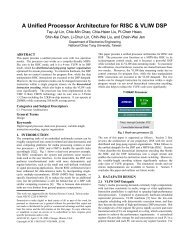
Design Methodologies of LTCC Bandpass Filters, Diplexer, and ...
Design Methodologies of LTCC Bandpass Filters, Diplexer, and ...
Design Methodologies of LTCC Bandpass Filters, Diplexer, and ...

Create successful ePaper yourself
Turn your PDF publications into a flip-book with our unique Google optimized e-Paper software.
718 IEEE TRANSACTIONS ON MICROWAVE THEORY AND TECHNIQUES, VOL. 54, NO. 2, FEBRUARY 2006<br />
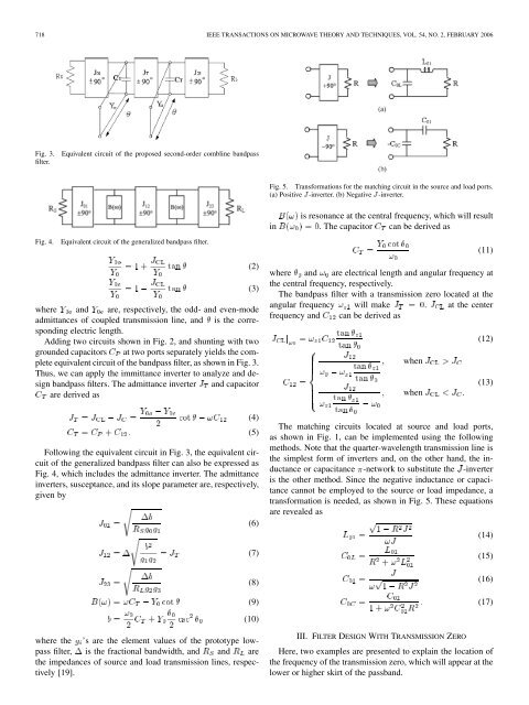
Fig. 3.<br />
filter.<br />
Equivalent circuit <strong>of</strong> the proposed second-order combline b<strong>and</strong>pass<br />
Fig. 5. Transformations for the matching circuit in the source <strong>and</strong> load ports.<br />
(a) Positive J-inverter. (b) Negative J-inverter.<br />
is resonance at the central frequency, which will result<br />
in . The capacitor can be derived as<br />
Fig. 4.<br />
Equivalent circuit <strong>of</strong> the generalized b<strong>and</strong>pass filter.<br />
where <strong>and</strong> are, respectively, the odd- <strong>and</strong> even-mode<br />
admittances <strong>of</strong> coupled transmission line, <strong>and</strong> is the corresponding<br />
electric length.<br />
Adding two circuits shown in Fig. 2, <strong>and</strong> shunting with two<br />
grounded capacitors at two ports separately yields the complete<br />
equivalent circuit <strong>of</strong> the b<strong>and</strong>pass filter, as shown in Fig. 3.<br />
Thus, we can apply the immittance inverter to analyze <strong>and</strong> design<br />
b<strong>and</strong>pass filters. The admittance inverter <strong>and</strong> capacitor<br />
are derived as<br />
Following the equivalent circuit in Fig. 3, the equivalent circuit<br />
<strong>of</strong> the generalized b<strong>and</strong>pass filter can also be expressed as<br />
Fig. 4, which includes the admittance inverter. The admittance<br />
inverters, susceptance, <strong>and</strong> its slope parameter are, respectively,<br />
given by<br />
(2)<br />
(3)<br />
(4)<br />
(5)<br />
(6)<br />
(7)<br />
(8)<br />
(9)<br />
(10)<br />
where the ’s are the element values <strong>of</strong> the prototype lowpass<br />
filter, is the fractional b<strong>and</strong>width, <strong>and</strong> <strong>and</strong> are<br />
the impedances <strong>of</strong> source <strong>and</strong> load transmission lines, respectively<br />
[19].<br />
(11)<br />
where <strong>and</strong> are electrical length <strong>and</strong> angular frequency at<br />
the central frequency, respectively.<br />
The b<strong>and</strong>pass filter with a transmission zero located at the<br />
angular frequency will make . at the center<br />
frequency <strong>and</strong> can be derived as<br />
when<br />
when<br />
(12)<br />
(13)<br />
The matching circuits located at source <strong>and</strong> load ports,<br />
as shown in Fig. 1, can be implemented using the following<br />
methods. Note that the quarter-wavelength transmission line is<br />
the simplest form <strong>of</strong> inverters <strong>and</strong>, on the other h<strong>and</strong>, the inductance<br />
or capacitance -network to substitute the -inverter<br />
is the other method. Since the negative inductance or capacitance<br />
cannot be employed to the source or load impedance, a<br />
transformation is needed, as shown in Fig. 5. These equations<br />
are revealed as<br />
III. FILTER DESIGN WITH TRANSMISSION ZERO<br />
(14)<br />
(15)<br />
(16)<br />
(17)<br />
Here, two examples are presented to explain the location <strong>of</strong><br />
the frequency <strong>of</strong> the transmission zero, which will appear at the<br />
lower or higher skirt <strong>of</strong> the passb<strong>and</strong>.