3B Scientific - Physics & Engineering Experiments
3B Scientific - Physics & Engineering Experiments
3B Scientific - Physics & Engineering Experiments

You also want an ePaper? Increase the reach of your titles
YUMPU automatically turns print PDFs into web optimized ePapers that Google loves.
UE3080300<br />
Electricity / Electronics<br />
Field effect transistors<br />
UE3080300<br />
basic PRINCIPLES<br />
A field effect transistor (FET) is a semiconductor component in which<br />
electric current passes through a channel and is controlled by an electric<br />
field acting perpendicular to the channel.<br />
FETs have three contacts, called source (S), drain (D) and gate (G) due to their<br />
respective functions. The channel comprises a conductive link between the<br />
source and the drain. If a voltage U DS is applied between source and drain,<br />
a drain current I D flows in the channel. The current is carried by carriers of<br />
only one polarity (unipolar transistors), i.e. electrons for an n-doped semiconductor<br />
channel and holes in a p-doped channel. The cross-section or the<br />
conductivity of the channel is controlled by the electric field perpendicular<br />
to the channel. To create this field, a gate voltage U GS is applied between<br />
the source and gate. The gate electrode is isolated from the channel by<br />
means of a reverse-biased pn junction or by an extra insulating layer (IGFET,<br />
MISFET, MOSFET). For insulated gate FETs the cross section of the channel<br />
is controlled by the expansion of the space-charge region of the junction,<br />
which is itself controlled by the perpendicular field. In order to ensure that<br />
the pn junction is always reverse-biased, i.e. specifically to make sure that<br />
there is no current at the gate, the gate voltage U GS and the drain-source<br />
voltage U DS must meet the following condition for an n-channel FET<br />
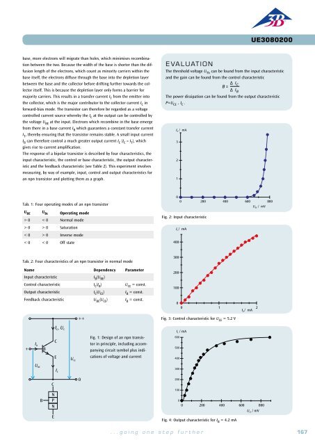
EVALUATION<br />
The measurements are plotted on a graph of I D against U DS for various<br />
values of the gate voltage U GS (Fig. 1). This should verify the shape of<br />
the characteristic showing how the drain current is controlled by the<br />
drain-source voltage and gate voltage.<br />
I D / mA<br />
8<br />
7<br />
6<br />
5<br />
4<br />
3<br />
U = 0 V<br />
GS<br />
U = -500 mV<br />
GS<br />
U = -1000 mV<br />
GS<br />
U = -1500 mV<br />
GS<br />
E X PERIMEN T<br />
PROCEDURE<br />
• Measure the drain voltage as a function<br />
of the drain current for various<br />
voltages at the gate.<br />
OBJECTIVE<br />
Measure the characteristics of a field effect transistor<br />
SUMMARY<br />
A field effect transistor (FET) is a semiconductor component in which electric current passes through<br />
a channel and is controlled by an electric field acting perpendicular to the channel. FETs have three<br />
contacts, called source, drain and gate due to their respective functions. If a voltage is applied between<br />
the source and the drain, then a drain current flows between the two. For small voltages between the<br />
drain and source, an FET acts like a simple ohmic resistor with a correspondingly linear characteristic.<br />
As the source-drain voltage increases, the channel becomes restricted and eventually is cut off entirely.<br />
The characteristic then enters an area of saturation. When the gate voltage is non-zero, the saturation<br />
value of the drain current decreases.<br />
(1a)<br />
and the following for a p-channel FET<br />
U GS<br />
≤ 0,U DS<br />
≥ 0<br />
(1b) U GS<br />
≥ 0,U DS<br />
≥ 0 .<br />
If the absolute value of the drain-source voltage |U DS | is small, the FET<br />
acts like an ohmic resistor with a correspondingly linear characteristic. As<br />
|U DS | increases, the channel is restricted in size because the reverse-bias<br />
voltage between the gate and the channel increases in the direction of the<br />
drain. The space-charge region near the drain is wider than that near the<br />
source, meaning that the channel is narrower near the drain than it is near<br />
the source. At a specific voltage where U DS = U p the width of the channel<br />
becomes zero and the drain current no longer increases even though the<br />
drain-source voltage is increased. The characteristic passes out of its ohmic<br />
region into a region of saturation.<br />
2<br />
1<br />
0<br />
0 1 2 3 4 5<br />
U D / V<br />
Fig. 1: Characteristic curve for FET with gate voltages 0 V (blue), -0.5 V (red),<br />
-1 V (green) and -1.5 V (turquoise)<br />
Required Apparatus<br />
Quantity Description Number<br />
1 Plug-In Board for Components 1012902<br />
1 Set of 10 Jumpers, P2W19 1012985<br />
1 Resistor 1 kΩ, 2 W, P2W19 1012916<br />
1 Resistor 470 Ω, 2 W, P2W19 1012914<br />
1 Resistor 47 kΩ, 0.5 W, P2W19 1012926<br />
1 Capacitor 470 µF, 16 V, P2W19 1012960<br />
The extent of the space-charge region and therefore the size of the channel<br />
can be controlled by means of the gate voltage. As long as the gate voltage<br />
is non-zero, the channel can undergo additional constriction, making the<br />
drain-source current smaller and, in particular, the saturation current lower.<br />
The channel remains blocked irrespective of the drain-source voltage U DS<br />
when |U GS | ≥ |U p |.<br />
The experiment involves measuring drain current I D as a function of drainsource<br />
voltage U DS for various gate voltages U GS .<br />
1 FET Transistor, BF 244, P4W50 1012978<br />
1 Silicon Diode, 1N 4007, P2W19 1012964<br />
1 Potentiometer 220 Ω, 3 W, P4W50 1012934<br />
1 AC/DC Power Supply 0 – 12 V, 3 A (230 V, 50/60 Hz) 1002776 or<br />
2<br />
AC/DC Power Supply 0 – 12 V, 3 A (115 V, 50/60 Hz) 1002775<br />
2 Analogue Multimeter AM50 1003073<br />
1 Set of 15 Experiment Leads, 75 cm 1 mm² 1002840<br />
168 <strong>3B</strong> <strong>Scientific</strong>® <strong>Experiments</strong><br />
...going one step further<br />
169