USB-4301 User's Guide
USB-4301 User's Guide
USB-4301 User's Guide

Create successful ePaper yourself
Turn your PDF publications into a flip-book with our unique Google optimized e-Paper software.
<strong>USB</strong>-<strong>4301</strong> <strong>User's</strong> <strong>Guide</strong><br />
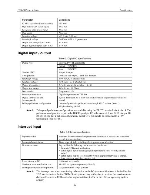
Specifications<br />
Parameter<br />
Conditions<br />
12 MHz crystal oscillator accuracy ±50 ppm<br />
High pulse width (clock input) 25 ns min<br />
Low pulse width (clock input) 25 ns min<br />
Gate width<br />
70 ns min<br />
Input low voltage<br />
-0.5 V min, 0.8V max<br />
Input high voltage<br />
2.0 V min, <strong>USB</strong> +5V power max<br />
Output low voltage @ IIl=4 mA 0.4 V max<br />
Output high voltage @ IIH= 4 mA 2.4 V min<br />
Digital input / output<br />
Table 2. Digital I/O specifications<br />
Digital type<br />
Discrete, 5V/TTL compatible<br />
Output: 74ACT373<br />
Input: 74ACT373<br />
Number of I/O<br />
8 input, 8 output<br />
Configuration<br />
1 bank of 8 as output, 1 bank of 8 as input<br />
Input high voltage<br />
2.0 V min,5.5 V absolute max<br />
Input low voltage<br />
0.8 V max, –0.5 V absolute min<br />
Output high voltage 3.3 volts min @ -24 mA (Vcc = 4.5 V)<br />
Output low voltage<br />
0.8 volts max @ 10 mA<br />
Data transfer<br />
Programmed I/O<br />
Power-up / reset state<br />
Digital outputs reset to TTL low<br />
Digital I/O transfer rate<br />
(system paced)<br />
System dependent, 33 to 1000 port reads/writes or single bit reads/writes per<br />
second.<br />
Pull-up/pull-down configuration User configurable for pull-up/-down through 47 kΩ resistor (Note 1).<br />
All pins floating (default)<br />
Note 1:<br />
Pull-up and pull-down configurations are available using the DI CTL terminal block pin 19. The<br />
pull-down configuration requires the DI CTL pin (pin 19) to be connected to a GND pin (pin 10,<br />
20, 38, or 48). For a pull-up configuration, the DI CTL pin should be connected to a +5V<br />
terminal pin (pin 8 or 18).<br />
Interrupt Input<br />
Table 3. Interrupt specifications<br />
Implementation<br />
Interrupts the microcontroller operation on the device to execute one or more of<br />
several firmware routines.<br />
Interrupt characteristics<br />
Rising edge (default) or falling edge triggered, user selectable<br />
Firmware routines<br />
Any or all of the following can be activated by the user:<br />
• Generate <strong>USB</strong> event notification<br />
• Latch digital inputs (Reading digital inputs returns most recently latched<br />
value.)<br />
• Latch digital outputs (Most recently written digital output value is latched.)<br />
• Save counts on any/all of counters 1-5.<br />
Event latency to PC<br />
1-33 ms (4 ms typical)<br />
Maximum event notification rate 33-1000 Hz (system dependent) (Note 2)<br />
Interrupt latency for latch operations 100 µs maximum (80 µs typical)<br />
Note 2:<br />
The interrupt rate, when transferring information to the PC (event notification), is limited by the<br />
<strong>USB</strong> to a theoretical limit of 1kHz. Some systems may not be able to achieve this maximum rate<br />
due to differences in <strong>USB</strong> controller implementation, traffic on the <strong>USB</strong>, or operating system<br />
activity.<br />
22