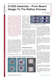
01005 Chip Components In A Lead-Free System - OnBoard ...
01005 Chip Components In A Lead-Free System - OnBoard ...
01005 Chip Components In A Lead-Free System - OnBoard ...

You also want an ePaper? Increase the reach of your titles
YUMPU automatically turns print PDFs into web optimized ePapers that Google loves.
SPECIAL Q U A L I T Y A REPORT<br />
S S U R A N C E LEAD-FREE ELECTRONICS<br />
ASSEMBLY<br />
<strong>01005</strong> <strong>Chip</strong> <strong>Components</strong><br />
<strong>In</strong> A <strong>Lead</strong>-<strong>Free</strong> <strong>System</strong><br />
A study was performed to understand<br />
the assembly constraints of<br />
the newest miniaturised package<br />
chip components, <strong>01005</strong> (or 0402<br />
metric). The study included all<br />
facets of surface mount assembly:<br />
pad design and location, printability<br />
of the small deposits, placement<br />
tolerances on the components,<br />
and reflow capability of the small,<br />
lead-free deposits in an air environment.<br />
This study was a joint effort<br />
between two manufacturers: a solder<br />
paste developer and a pick and<br />
place machine supplier.<br />
The study tested multiple solder<br />
deposit sizes as part of an effort to<br />
characterise the repeatability of the<br />
paste prints and the paste’s reflow<br />
fusion capability in air. It also tested<br />
several component placement<br />
orientations and offsets, and multiple<br />
padstacks. The result shows<br />
strong feasibility of <strong>01005</strong> devices<br />
in modern assembly systems, and<br />
discusses the parameters that produced<br />
the best results in the system<br />
under consideration.<br />
Miniaturisation in electronic products<br />
continually drives the need for<br />
smaller and smaller component<br />
packages. Smaller components<br />
bring solutions to designers seeking<br />
smaller form factors, but they<br />
also bring challenges to the assemblers.<br />
Several years ago, the package size<br />
known as 0201 (Imperial) or 0603<br />
(metric) presented new challenges<br />
to assemblers. Many studies were<br />
performed to show the feasibility.<br />
Now, the package size known as<br />
<strong>01005</strong> (Imperial) or 0402 (metric) is<br />
available. The 0402 is approximately<br />
one-fourth the size of an 0603. The<br />
relative sizes of chip components<br />
are shown in Figure 1.<br />
Experimental setup<br />
by Chrys Shea, Dr. Leszek Hozer, Hitoshi Kida, Mutsuharu Tsunoda,<br />
Cookson Electronics Assembly Materials<br />
Figure 1 - Relative sizes of chip<br />
components<br />
Four major tests were included in<br />
the experiment. Characteristics<br />
that were tested for included<br />
• Printability<br />
• Reflow capability<br />
• Placement accuracy<br />
• Self-alignment<br />
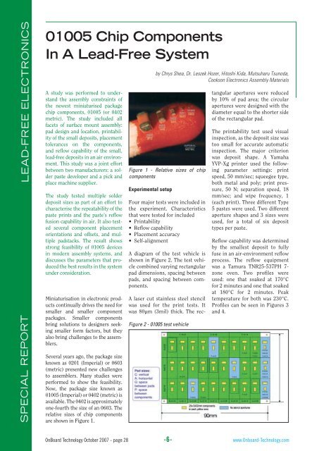
A diagram of the test vehicle is<br />
shown in Figure 2. The test vehicle<br />
combined varying rectangular<br />
pad dimensions, spacing between<br />
pads, and spacing between components.<br />
Figure 2 - <strong>01005</strong> test vehicle<br />
A laser cut stainless steel stencil<br />
was used for the print tests. It<br />
was 80µm (3mil) thick. The rectangular<br />
apertures were reduced<br />
by 10% of pad area; the circular<br />
apertures were designed with the<br />
diameter equal to the shorter side<br />
of the rectangular pad.<br />
The printability test used visual<br />
inspection, as the deposit size was<br />
too small for accurate automatic<br />
inspection. The major criterion<br />
was deposit shape. A Yamaha<br />
YVP-Xg printer used the following<br />
parameter settings: print<br />
speed, 50 mm/sec; squeegee type,<br />
both metal and poly; print pressure,<br />
50 N; separation speed, 18<br />
mm/sec; and wipe frequency, 1<br />
(each print). Three different Type<br />
5 pastes were used. Two different<br />
aperture shapes and 3 sizes were<br />
used, for a total of six deposit<br />
types per paste.<br />
Reflow capability was determined<br />
by the smallest deposit to fully<br />
fuse in an air-environment reflow<br />
process. The reflow equipment<br />
was a Tamura TNR25-537PH 7-<br />
zone oven. Two profiles were<br />
used: one that soaked at 170°C<br />
for 2 minutes and one that soaked<br />
at 180°C for 2 minutes. Peak<br />
temperature for both was 230°C.<br />
Profiles can be seen in Figures 3<br />
and 4.<br />
<strong>OnBoard</strong> Technology October 2007 - page 28<br />
-6-<br />
www.Onboard-Technology.com
Figure 3 - 170°C soak profile<br />
A chip placing test was performed<br />
to determine the necessary accuracy<br />
of the placer and explore<br />
the limits of the process window<br />
with respect to defects and selfcentring.<br />
A Yamaha YV88Xg was<br />
used to perform the tests. It has<br />
a mounting accuracy of 0.05mm<br />
(2mil). Placement pressure, location<br />
and rotation were varied.<br />
Placements were programmed<br />
with each combination of following<br />
offsets: 0 and 0.05mm in X<br />
and Y; -0.2mm, 0, and +0.2mm in<br />
Z, and 0 – 25 degrees theta in 5<br />
degree increments. Tolerances of<br />
the test boards, stencil, and components<br />
that were used in this<br />
test are shown in Figure 5.<br />
Results<br />
Three Type 5 <strong>Lead</strong>-<strong>Free</strong> pastes<br />
were tested. They were labelled<br />
A, B and C. Paste C provided the<br />
best printability. Its smallest acceptable<br />
print size was 0.16mm<br />
(6.3mil) square or 0.18mm<br />
(7.1mil) round with metal squeegee,<br />
and 0.13mm (5.1mil) square<br />
or 0.14mm (5.5 mil) round with<br />
rubber squeegee. Photographs<br />
of the smallest acceptable prints<br />
with metal squeegee with Paste C<br />
are shown in Figures 6 and 7.<br />
Of the three pastes tested for reflow<br />
characteristics, Paste C also<br />
performed the best, with the finest<br />
features to completely reflow in<br />
air sized 0.16mm (6.3mil) square<br />
or 0.18mm (7.1mil) round. This<br />
coincided with the finest feature<br />
this paste could repeatably print.<br />
Photos of reflowed deposits are<br />
shown in Figures 8 and 9.<br />
Figure 4 - 180°C soak profile<br />
Paste C exhibited the best print<br />
and reflow characteristics, therefore<br />
it was used for the remainder<br />
of the tests.<br />
A nitrogen reflow environment<br />
was not included with this test.<br />
It is hypothesised that smaller<br />
features, on the order of 0.13mm<br />
(5mil) square and 0.14mm<br />
(5.5mil) round would reflow under<br />
nitrogen. Recall that the smallest<br />
acceptable print deposit size was<br />
0.16 and 0.18mm. Therefore there<br />
was no need to explore reflow<br />
properties of a deposit size that<br />
could not be repeatably printed.<br />
Placement tests showed that the<br />
current capability of the equipment<br />
is sufficient for 0402/<strong>01005</strong><br />
placement. Even offsets of 0.05mm<br />
(2mil) in both X and Y resulted in<br />
Figure 6 - 0.16mm (6.2mil) square<br />
features<br />
Figure 8 - 0.16mm (6.3 mil) square<br />
deposits after<br />
Placement pressure of -0.2mm Z<br />
was the weakest force tested, and<br />
LEAD-FREE ELECTRONICS<br />
ASSEMBLY<br />
Figure 5 - Tolerance stack up of test assembly<br />
components<br />
Figure 7 - 0.18mm (7.1mil) round<br />
features<br />
Figure 9 - 0.18mm (7.1mil) round<br />
deposits after reflow<br />
Q U A L I T Y A S S U R A N C E<br />
www.Onboard-Technology.com<br />
centred components after reflow.<br />
Figure 10 shows the post-reflow<br />
state of the offset components.<br />
Theta offsets as much as 25° also<br />
self-centred in the reflow process;<br />
however, offsets of 10° or less are<br />
preferred. Figures 11 and 12 show<br />
10° rotations before and after reflow.<br />
-7-<br />
<strong>OnBoard</strong> Technology October 2007 - page 29
SPECIAL Q U A L I T Y A REPORT<br />
S S U R A N C E LEAD-FREE ELECTRONICS<br />
ASSEMBLY<br />
Figure 10 - Post-reflow alignment<br />
of 0402/<strong>01005</strong> devices placed with<br />
0.05mm offsets in X and Y<br />
Figure 11 - 0402/<strong>01005</strong> components<br />
placed with 10° theta offset<br />
Figure 13 - 0402/<strong>01005</strong> component<br />
“floating” on solder due to<br />
insufficient placement pressure.<br />
The solder reflowed, but did not<br />
wet to the component floating on<br />
top of it<br />
Figure 14 - 0402/<strong>01005</strong> components<br />
placed with 0.07mm gap between<br />
pads. No solder bridges observed<br />
With respect to design guidelines<br />
for the PWB itself, this experishowed<br />
good placement characteristics<br />
with very little paste<br />
spread. Placement pressures this<br />
light require good tack force. The<br />
paste in this test had a tack force<br />
of 100fg, which appeared to be<br />
sufficient to maintain the components’<br />
positions throughout the<br />
normal conveying process on the<br />
assembly equipment.<br />
This force may be a little light, as<br />
several components “floated” on<br />
top the solder during the reflow<br />
process. An example is shown in<br />
Figure 13.<br />
The next larger force, 0mm Z,<br />
did squeeze some paste out from<br />
Figure 12 - 0402/<strong>01005</strong> components<br />
that were rotated 10° theta selfcentred<br />
during the reflow process<br />
under the component, but eliminated<br />
floating issues. The largest<br />
placement force, +0.2mm<br />
Z, squeezed too much paste out<br />
from under the component. This<br />
effectively broke up the solder deposits,<br />
making them smaller than<br />
their reflow capability, and left<br />
some paste unfused.<br />
Observations made during this<br />
test included mispicks, where the<br />
component was left in the tape<br />
pocket, but once a component<br />
was successfully picked, no issues<br />
were noted with vision alignment<br />
or dropping of the devices prior<br />
to placement. No tombstones or<br />
blown off components were observed.<br />
Figure 15 - 0402/<strong>01005</strong> components<br />
placed with 0.05mm gaps between<br />
pads. Notice the solder bridges<br />
ment showed a minimum end-toend<br />
spacing of 0.07 mm (2.8mil).<br />
Figures 14 and 15 show the results<br />
of pad spacing at 0.07mm<br />
and 0.05mm.<br />
Conclusion<br />
Technological feasibility of assembling<br />
component package<br />
sizes known as <strong>01005</strong> Imperial<br />
or 0402 metric has been proven<br />
in a lead-free alloy system. Type<br />
5 solder pastes were used with<br />
demanding, extended-soak reflow<br />
profiles.<br />
Typical assembly equipment was<br />
used. With the exception of a<br />
special nozzle size for the component,<br />
no modifications were<br />
made to the printer, chip placer,<br />
or reflow oven. Typical print parameters<br />
were used with a standard<br />
laser cut stencil.<br />
Of three pastes, the best performer<br />
in both print and reflow<br />
characteristics was candidate<br />
C, which is now commercially<br />
known as Alpha OM-325. The<br />
finest features to print repeatably<br />
and reflow completely in air<br />
were 0.16mm (6.3mil) square and<br />
0.18mm (7.1mil) round.<br />
<strong>In</strong>itial definition of the process<br />
window shows that with the proper<br />
material set, the components<br />
may be placed off-centre by as<br />
much as 0.05mm (2mil) in both<br />
X and Y axes. It may also be misplaced<br />
by up to 25° in theta, but<br />
less than 10° is preferred.<br />
Placement pressure is critical.<br />
Too little pressure may result in<br />
component floating. Too much<br />
pressure may cause solder deposits<br />
to break up and not fully fuse<br />
in reflow. Gross misplacement of<br />
the components may also have<br />
the same effect on reflow characteristics.<br />
Component locations on the circuit<br />
board should be spaced no<br />
closer than 0.07mm (2.8mil) to<br />
eliminate the defect mode of solder<br />
bridging.<br />
<strong>OnBoard</strong> Technology October 2007 - page 30<br />
-8-<br />
www.Onboard-Technology.com