Military Embedded Systems Summer 2006
Military Embedded Systems Summer 2006
Military Embedded Systems Summer 2006

You also want an ePaper? Increase the reach of your titles
YUMPU automatically turns print PDFs into web optimized ePapers that Google loves.
Hardware<br />
Reconfigurable FPGAs<br />
Board vendor FPGA toolkits make<br />
or break your project<br />
By Mark Littlefield<br />
FPGAs dramatically accelerate DSP<br />
designs while bringing reconfigurability<br />
to the battlefield. But to wring out<br />
performance, ease-of-use, and overall<br />
program benefits, a design toolkit is<br />
needed. Better choose wisely.<br />
Increasingly, the military community<br />
is recognizing that there is a class<br />
of signal processing that is now best<br />
accomplished via a reconfigurable computing<br />
implementation instead of the<br />
traditional method of software running<br />
on microprocessors. Modern Field Programmable<br />
Gate Arrays (FPGAs) have<br />
reached a level of density, speed, and cost<br />
such that system designers can now often<br />
achieve a tenfold reduction in size and<br />
power when compared with the traditional<br />
microprocessor-based approach. The<br />
power of FPGAs stems from the<br />
opportunity to parallelize operations that<br />
a microprocessor must do sequentially.<br />
For many signal processing designers,<br />
the question is not whether the use of<br />
FPGAs will result in higher performance<br />
– performance/power/cost – but whether<br />
the R&D investment will pay off. The<br />
simple fact is that developing signal<br />
processing functions in FPGAs has high<br />
technical risk, which can result in cost<br />
and schedule overruns.<br />
When selecting a COTS board level<br />
product, a system integrator should<br />
be aware that the board vendor FPGA<br />
supporting toolkit will play a large role<br />
in reducing (or not) this technical risk.<br />
Herein, we will acquaint the reader with<br />
the nature of such tools and their effect on<br />
the cost of developing an FPGA compute<br />
solution.<br />
What is an FPGA toolkit?<br />
In our context, an FPGA toolkit is the<br />
collection of supporting IP (VHDL<br />
designs) and other software components<br />
that are offered for use by the vendor of<br />
a board level product. We are not talking<br />
about the synthesis and simulation tools<br />
that are the domain of the FPGA silicon<br />
vendors and other tool specialists.<br />
The components of an FPGA board<br />
toolkit fall into four categories:<br />
• IP designs to control hardware<br />
features, for example, an SDRAM<br />
controller<br />
• IP infrastructure to connect IP blocks<br />
together<br />
• Software for system services, data<br />
movement, and general system<br />
integration<br />
• Simulation and test<br />
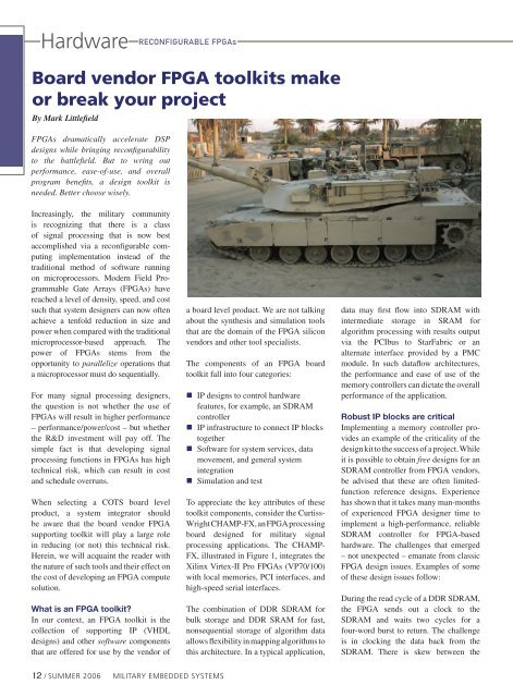
To appreciate the key attributes of these<br />
toolkit components, consider the Curtiss-<br />
Wright CHAMP-FX, an FPGA processing<br />
board designed for military signal<br />
processing applications. The CHAMP-<br />
FX, illustrated in Figure 1, integrates the<br />
Xilinx Virtex-II Pro FPGAs (VP70/100)<br />
with local memories, PCI interfaces, and<br />
high-speed serial interfaces.<br />
The combination of DDR SDRAM for<br />
bulk storage and DDR SRAM for fast,<br />
nonsequential storage of algorithm data<br />
allows flexibility in mapping algorithms to<br />
this architecture. In a typical application,<br />
data may first flow into SDRAM with<br />
intermediate storage in SRAM for<br />
algorithm processing with results output<br />
via the PCIbus to StarFabric or an<br />
alternate interface provided by a PMC<br />
module. In such dataflow architectures,<br />
the performance and ease of use of the<br />
memory controllers can dictate the overall<br />
performance of the application.<br />
Robust IP blocks are critical<br />
Implementing a memory controller provides<br />
an example of the criticality of the<br />
design kit to the success of a project. While<br />
it is possible to obtain free designs for an<br />
SDRAM controller from FPGA vendors,<br />
be advised that these are often limitedfunction<br />
reference designs. Experience<br />
has shown that it takes many man-months<br />
of experienced FPGA designer time to<br />
implement a high-performance, reliable<br />
SDRAM controller for FPGA-based<br />
hardware. The challenges that emerged<br />
– not unexpected – emanate from classic<br />
FPGA design issues. Examples of some<br />
of these design issues follow:<br />
During the read cycle of a DDR SDRAM,<br />
the FPGA sends out a clock to the<br />
SDRAM and waits two cycles for a<br />
four-word burst to return. The challenge<br />
is in clocking the data back from the<br />
SDRAM. There is skew between the<br />
12 / SUMMER <strong>2006</strong> <strong>Military</strong> EMBEDDED SYSTEMS