Military Embedded Systems Summer 2006
Military Embedded Systems Summer 2006
Military Embedded Systems Summer 2006

You also want an ePaper? Increase the reach of your titles
YUMPU automatically turns print PDFs into web optimized ePapers that Google loves.
Hardware<br />
Reconfigurable FPGAs<br />
Design strategies for an FPGAbased<br />
256-channel digital<br />
down converter<br />
By Rodger H. Hosking<br />
FPGAs can replace traditional ASIC-based<br />
digital down converters in high channel<br />
count Software-Defined Radios. Their<br />
inherent parallelism allows multiple digital<br />
receiver channels per chip, and available<br />
COTS IP cores can be used to realize up to<br />
256 independently controlled channels in a<br />
Xilinx Virtex family FPGA.<br />
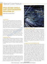
WideBIN<br />
Complex<br />
Input<br />
As Software-Defined Radio technology<br />
further penetrates large communication<br />
systems for battlefield military radio<br />
networks, commercial wireless systems,<br />
manned and unmanned aerial vehicles, and<br />
monitoring facilities for SIGINT and COMINT, the need to<br />
accommodate a large number of agile frequency channels for<br />
radio receivers is quite apparent. In each of these applications,<br />
the same critical metrics apply: size, weight, power, and cost for<br />
each receiver channel.<br />
Traditional Digital Down Converter (DDC) ASIC devices<br />
feature only one to four channels per chip, and straightforward<br />
implementations of DDCs in FPGAs consume a significant<br />
percentage of available resources. A new approach to DDC<br />
design takes advantage of the parallelism of FPGAs to create a<br />
highly efficient architecture for multichannel receivers.<br />
Basics of digital down converters<br />
DDCs, often called digital receivers, perform the two essential<br />
software radio functions: frequency translation and channel<br />
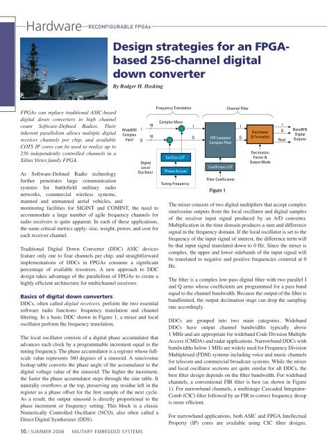
filtering. In a basic DDC shown in Figure 1, a mixer and local<br />
oscillator perform the frequency translation.<br />
The local oscillator consists of a digital phase accumulator that<br />
advances each clock by a programmable increment equal to the<br />
tuning frequency. The phase accumulator is a register whose fullscale<br />
value represents 360 degrees of a sinusoid. A sine/cosine<br />
lookup table converts the phase angle of the accumulator to the<br />
digital voltage value of the sinusoid. The higher the increment,<br />
the faster the phase accumulator steps through the sine table. It<br />
naturally overflows at the top, preserving any residue left in the<br />
register as a phase offset for the first sample of the next cycle.<br />
As a result, the output sinusoid is directly proportional to the<br />
phase increment or frequency setting. This block is a classic<br />
Numerically Controlled Oscillator (NCO), also often called a<br />
Direct Digital Synthesizer (DDS).<br />
16 / SUMMER <strong>2006</strong> <strong>Military</strong> EMBEDDED SYSTEMS<br />
I<br />
Q<br />
16<br />
16<br />
Digital<br />
Local<br />
Oscillator<br />
Frequency Translation<br />
Complex Mixer<br />
Sin/Cos LUT<br />
Phase Accum<br />
Tuning Frequency<br />
I<br />
Q<br />
FIR Lowpass<br />
Complex Filter<br />
Coefficient LUT<br />
Filter Coefficients<br />
Figure 1<br />
Channel Filter<br />
Decimator<br />
& Formatter<br />
The mixer consists of two digital multipliers that accept complex<br />
sine/cosine outputs from the local oscillator and digital samples<br />
of the receiver input signal produced by an A/D converter.<br />
Multiplication in the time domain produces a sum and difference<br />
signal in the frequency domain. If the local oscillator is set to the<br />
frequency of the input signal of interest, the difference term will<br />
be that input signal translated down to 0 Hz. Since the mixer is<br />
complex, the upper and lower sidebands of the input signal will<br />
be translated to negative and positive frequencies centered at 0<br />
Hz.<br />
The filter is a complex low-pass digital filter with two parallel I<br />
and Q arms whose coefficients are programmed for a pass band<br />
equal to the channel bandwidth. Because the output of the filter is<br />
bandlimited, the output decimation stage can drop the sampling<br />
rate accordingly.<br />
DDCs are grouped into two main categories. Wideband<br />
DDCs have output channel bandwidths typically above<br />
1 MHz and are appropriate for wideband Code Division Multiple<br />
Access (CMDA) and radar applications. Narrowband DDCs with<br />
bandwidths below 1 MHz are widely used for Frequency Division<br />
Multiplexed (FDM) systems including voice and music channels<br />
for telecom and commercial broadcast systems. While the mixer<br />
and local oscillator sections are quite similar for all DDCs, the<br />
best filter design depends on the filter bandwidth. For wideband<br />
channels, a conventional FIR filter is best (as shown in Figure<br />
1). For narrowband channels, a multistage Cascaded Integrator-<br />
Comb (CIC) filter followed by an FIR to correct frequency droop<br />
is more efficient.<br />
For narrowband applications, both ASIC and FPGA Intellectual<br />
Property (IP) cores are available using CIC filter designs.<br />
I<br />
Q<br />
Decimation<br />
Factor &<br />
Output Mode<br />
I<br />
Q<br />
Real<br />
BaseBIN<br />
Digital<br />
Outputs