Military Embedded Systems Summer 2006
Military Embedded Systems Summer 2006
Military Embedded Systems Summer 2006

Create successful ePaper yourself
Turn your PDF publications into a flip-book with our unique Google optimized e-Paper software.
Hardware<br />
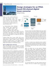
Reconfigurable FPGAs<br />
Commercial ASICs feature as many as four channels per chip,<br />
like the popular Texas Instruments/Graychip GC4016.<br />
IP core DDCs, like the LogiCore DDC from Xilinx for its<br />
Virtex-II Pro, can be scaled for various levels of Spurious-<br />
Free Dynamic Range (SFDR) performance to use more or less<br />
of the available resources. For example, a complex DDC with<br />
84 dB SFDR consumes approximately 1,700 slices. In a mid-sized<br />
FPGA device with 24,000 available slices, only about 14 DDC<br />
channels can be accommodated. For applications requiring<br />
several dozen or even hundreds of channels, this approach can<br />
become impractical.<br />
Channelizers<br />
Because of the extremely fine resolution of its NCO tuning<br />
frequency, a true DDC can translate any input frequency<br />
component down to 0 Hz, often with 32-bit accuracy. This ability<br />
makes DDCs ideal for applications that require precise changes<br />
in tuning such as in continuous Doppler correction for satellite<br />
tracking systems.<br />
However, in other applications, a channelizer approach may<br />
be sufficient. This is a bank of equally spaced, fixed frequency<br />
band pass filters whose outputs are translated to baseband (0 Hz).<br />
One crude example of a channelizer familiar to everyone is a<br />
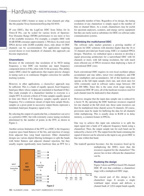
simple FFT. It converts a block of N time samples equally spaced<br />
in time into block of N frequency samples equally spaced in<br />
frequency. For a continuous stream of input time sample blocks,<br />
samples at a given point in successive output blocks represent a<br />
translated, band pass frequency signal or bin.<br />
By selecting the output of a particular bin, a channelizer can serve<br />
as a primitive DDC, but with extremely coarse tuning resolution<br />
determined by the number of points in the FFT, as shown in<br />
Figure 2.<br />
Another serious limitation of the FFT as a DDC is the frequency<br />
response (pass band flatness) of the bin, and rejection of energy<br />
from adjacent bins (stop band rejection). Other channelizer<br />
designs use various digital filtering techniques to split the bands<br />
with better flatness and adjacent channel rejection, but they<br />
usually require significantly more hardware than an FFT for a<br />
BIN 1<br />
BIN 2<br />
BIN 3<br />
comparable number of bins. Regardless of its design, the tuning<br />
resolution of any channelizer is simply equal to the number of<br />
bins or channel filters. As a result, channelizers may be useful<br />
for spectrum analyzers, scanners, and energy survey equipment<br />
but they are rarely used as substitutes for DDCs in software radio<br />
communication systems.<br />
Rethinking the multichannel DDC<br />
The software radio market generates a growing number of<br />
requests for DDC solutions with densities higher than the 16 or<br />
32 channels provided per board using ASICs or standard FPGA<br />
designs. Therefore, we embarked upon a mission to develop a<br />
signal processing architecture for a narrowband DDC with 64<br />
channels or more, with full tuning resolution, but with much<br />
more efficient use of FPGA resources than deploying a farm of<br />
conventional DDC cores.<br />
Each conventional DDC requires its own local oscillator (phase<br />
accumulator and sine table), mixer (two multipliers), and FIR<br />
filter (multipliers and accumulators). All of this hardware must<br />
operate at the full input sample clock rate, and clock rates for<br />
A/Ds commonly used in software radios range between 100<br />
and 200 MHz. Since this is the same clock range rating for<br />
commercial DDC IP cores, all of the hardware resources used for<br />
each channel must be dedicated to that channel.<br />
However, imagine that the input data sample rate is reduced by<br />
a factor N. By operating the DDC hardware resources required<br />
for one channel at the full clock rate, those same resources can<br />
then be multiplexed (time shared) across N channels. Of course,<br />
provisions must be made for buffering the data for all channels<br />
while multiplexing. This is usually done in RAM or in delay<br />
memory, a common feature in FPGAs.<br />
One way to achieve this input rate reduction is to split the<br />
input signal into a bank of N adjacent frequency bands using a<br />
channelizer. Then, the output sample rate for each band can be<br />
reduced by a factor of N. The output from the band containing the<br />
signal of interest can be selected as the input to any given DDC to<br />
fine tune within that band.<br />
The tradeoff question becomes: Are the resources freed up by<br />
multiplexing the DDCs more than the<br />
resources required for the channelizer? The<br />
answer lies in how efficient the channelizer<br />
can be.<br />
INPUT<br />
Sample Rate<br />
= Fs<br />
FFT<br />
1024<br />
POINTS<br />
Sample Rate<br />
= Fs/1024<br />
Amplitude<br />
Realizing the design<br />
Figure 3 shows an FPGA-based 256-channel<br />
DDC IP core that combines a channelizer<br />
stage with a multiplexed DDC stage.<br />
BIN 1022<br />
BIN 1023<br />
BIN 1024<br />
Figure 2<br />
BIN<br />
n<br />
BIN<br />
n+1<br />
BIN<br />
n+2<br />
BIN<br />
n+3<br />
Freq<br />
The crucial part of this design is the<br />
channelizer stage. It accepts a single<br />
wideband input stream and delivers a<br />
channel bank of 1,024 output bands equally<br />
18 / SUMMER <strong>2006</strong> <strong>Military</strong> EMBEDDED SYSTEMS