Military Embedded Systems Summer 2006
Military Embedded Systems Summer 2006
Military Embedded Systems Summer 2006

You also want an ePaper? Increase the reach of your titles
YUMPU automatically turns print PDFs into web optimized ePapers that Google loves.
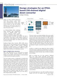
Reconfigurable FPGAs<br />
Hardware<br />
spaced in frequency, but with significant<br />
overlap between adjacent bands.<br />
The output sample rate of each band<br />
equals the input sample rate (Fs) divided<br />
by 256, rather than 1,024, as would be<br />
expected with a simple FFT. In fact,<br />
inside the channelizer are four highspeed<br />
1,024-point FFTs running in<br />
parallel using a proprietary windowing<br />
and overlap processing technique.<br />
The outputs of the four separate FFTs<br />
deliver samples at a rate of Fs/1024.<br />
These outputs are combined to form a<br />
single output at a sample rate of Fs/256,<br />
supporting the wider bandwidth that will<br />
sufficiently overlap adjacent bands.<br />
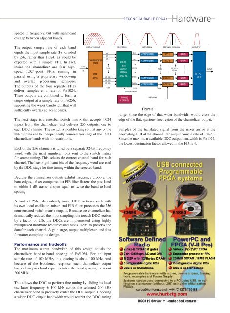
The next stage is a crossbar switch matrix that accepts 1,024<br />
inputs from the channelizer and delivers 256 outputs, one to<br />
each DDC channel. The switch is nonblocking so that any of the<br />
256 outputs can be independently sourced from any of the 1,024<br />
channelizer bands with no restrictions.<br />
Each of the 256 channels is tuned by a separate 32-bit frequency<br />
word, with the most significant bits sent to the switch matrix<br />
for coarse tuning. This selects the correct channel band for each<br />
channel. The least significant bits of the frequency word are used<br />
by the DDC stage for fine tuning within the selected band.<br />
Because the channelizer outputs exhibit frequency droop at the<br />
band edges, a fixed compensation FIR filter flattens the pass band<br />
to within 1 dB across a span equal to twice the band-to-band<br />
spacing.<br />
INPUT<br />
FS<br />
OVERLAPPING BINS SELECTED BIN FLATTENED BIN DDC TUNING WITHIN BIN<br />
DDC OUTPUT<br />
CHANNELIZATION<br />
STAGE<br />
1024<br />
BINS<br />
BIN 1<br />
BIN 2<br />
BIN 3<br />
FS/256<br />
BIN 1022<br />
BIN 1023<br />
BIN 1024<br />
CROSS<br />
BAR<br />
SWITCH<br />
MATRIX<br />
1024 x 256<br />
TUNING<br />
CONTROL<br />
CH 1<br />
CH 2<br />
FS/256<br />
CH 255<br />
CH 256<br />
COARSE TUNING<br />
COMP FILTER<br />
FS/256 FS/256 FS/256<br />
FINE TUNING<br />
DDC 1<br />
GAIN<br />
COMP FILTER DDC 2 GAIN<br />
COMP FILTER DDC 255 GAIN<br />
COMP FILTER DDC 256 GAIN<br />
Figure 3<br />
FS/256<br />
FS/1024 to<br />
FS/9984<br />
OUTPUT<br />
range, since the edge of that wider bandwidth would cross the<br />
edge of the flat, spurious-free region of the channelizer output.<br />
Samples of the translated signal from the mixer arrive at the<br />
decimating FIR at the channelizer output sample rate of Fs/256.<br />
Since the maximum available DDC output bandwidth is Fs/1024,<br />
the lowest decimation factor allowed in the FIR is 4.<br />
MUX<br />
OUTPUT<br />
A bank of 256 independently tuned DDC sections, each with<br />
its own local oscillator, mixer, and FIR filter, processes the 256<br />
compensated switch matrix outputs. Because the channelizer has<br />
dramatically reduced the input sampling rate to each DDC section<br />
by a factor of 256, the DDCs are implemented using highly<br />
multiplexed hardware resources and block RAM to preserve the<br />
data for each channel. A gain stage, output multiplexer, and data<br />
formatter complete the design.<br />
Performance and tradeoffs<br />
The maximum output bandwidth of this design equals the<br />
channelizer band-to-band spacing of Fs/1024. For an input<br />
sample rate of 100 MHz, this spacing is about 100 kHz. And<br />
because of the broadened response, each channelizer output<br />
has a clean pass band equal to twice the band spacing, or about<br />
200 MHz.<br />
This allows the DDC to perform fine tuning by sliding its local<br />
oscillator frequency ± 100 kHz across the selected 200 kHz<br />
channelizer band to precisely center the DDC output. Choosing<br />
a wider DDC output bandwidth would restrict the DDC tuning<br />
RSC# 19 @www.mil-embedded.com/rsc