04. 01 Directory chapter 04 Connectors with press-in termination
04. 01 Directory chapter 04 Connectors with press-in termination
04. 01 Directory chapter 04 Connectors with press-in termination

Create successful ePaper yourself
Turn your PDF publications into a flip-book with our unique Google optimized e-Paper software.
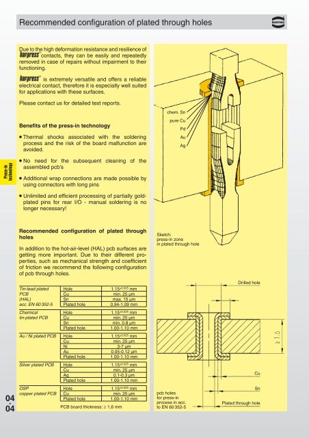
Recommended configuration of plated through holes<br />
Due to the high deformation resistance and resilience of<br />
contacts, they can be easily and repeatedly<br />
removed <strong>in</strong> case of repairs <strong>with</strong>out impairment to their<br />
function<strong>in</strong>g.<br />
is extremely versatile and offers a reliable<br />
electrical contact, therefore it is especially well suited<br />
for applications <strong>with</strong> these surfaces.<br />
Please contact us for detailed test reports.<br />
chem. Sn<br />
Benefits of the <strong>press</strong>-<strong>in</strong> technology<br />
l Thermal shocks associated <strong>with</strong> the solder<strong>in</strong>g<br />
process and the risk of the board malfunction are<br />
avoided.<br />
pure Cu<br />
Pd<br />
Au<br />
Ag<br />
Press-<strong>in</strong><br />
technology<br />
l No need for the subsequent clean<strong>in</strong>g of the<br />
assembled pcb’s<br />
l Additional wrap connections are made possible by<br />
us<strong>in</strong>g connectors <strong>with</strong> long p<strong>in</strong>s<br />
l Unlimited and efficient process<strong>in</strong>g of partially goldplated<br />
p<strong>in</strong>s for rear I/O - manual solder<strong>in</strong>g is no<br />
longer necessary!<br />
Recommended configuration of plated through<br />
holes<br />
In addition to the hot-air-level (HAL) pcb surfaces are<br />
gett<strong>in</strong>g more important. Due to their different properties,<br />
such as mechanical strength and coefficient<br />
of friction we recommend the follow<strong>in</strong>g configuration<br />
of pcb through holes.<br />
Sketch:<br />
<strong>press</strong>-<strong>in</strong> zone<br />
<strong>in</strong> plated through hole<br />
T<strong>in</strong>-lead plated Hole 1.15 ±0.025 mm<br />
PCB Cu m<strong>in</strong>. 25 µm<br />
(HAL) Sn max. 15 µm<br />
acc. EN 60 352-5 Plated hole 0.94-1.09 mm<br />
Drilled hole<br />
Chemical Hole 1.15 ±0.025 mm<br />
t<strong>in</strong>-plated PCB Cu m<strong>in</strong>. 25 µm<br />
Sn m<strong>in</strong>. 0.8 µm<br />
Plated hole<br />
1.00-1.10 mm<br />
Au / Ni plated PCB Hole 1.15 ±0.025 mm<br />
Cu m<strong>in</strong>. 25 µm<br />
Ni 3-7 µm<br />
Au 0.05-0.12 µm<br />
Plated hole<br />
1.00-1.10 mm<br />
Silver plated PCB Hole 1.15 ±0.025 mm<br />
Cu m<strong>in</strong>. 25 µm<br />
Ag 0.1-0.3 µm<br />
Plated hole<br />
1.00-1.10 mm<br />
Cu<br />
<strong>04</strong> .<br />
<strong>04</strong><br />
OSP Hole 1.15 ±0.025 mm<br />
copper plated PCB Cu m<strong>in</strong>. 25 µm<br />
Plated hole<br />
1.00-1.10 mm<br />
PCB board thickness: ≥ 1,6 mm<br />
pcb holes<br />
for <strong>press</strong>-<strong>in</strong><br />
process <strong>in</strong> acc.<br />
to EN 60 352-5<br />
Sn<br />
Plated through hole