ARM PrimeCell Synchronous Serial Port (PL022) Technical ...
ARM PrimeCell Synchronous Serial Port (PL022) Technical ...
ARM PrimeCell Synchronous Serial Port (PL022) Technical ...

You also want an ePaper? Increase the reach of your titles
YUMPU automatically turns print PDFs into web optimized ePapers that Google loves.
Functional Overview<br />
SSPCLKOUT/<br />
SSPCLKIN<br />
SSPFSSOUT/<br />
SSPFSSIN<br />
SSPTXD/<br />
LSB<br />
SSPRXD<br />
nSSPOE (=0)<br />
MSB LSB MSB<br />
4 to 16 bits<br />
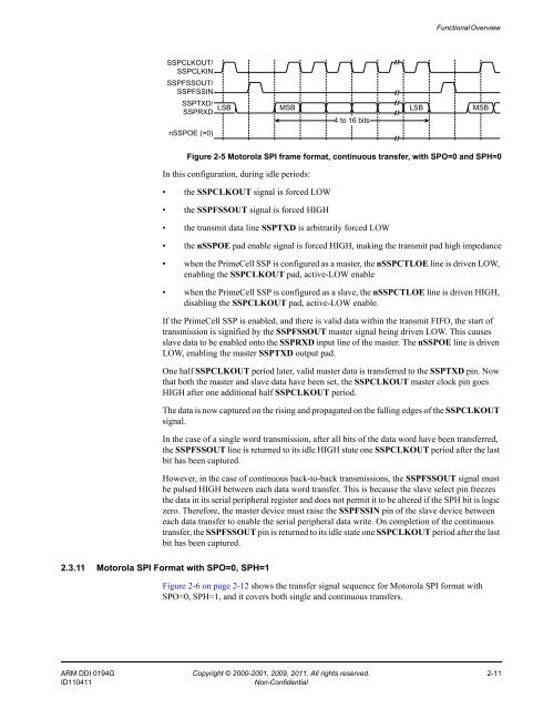
Figure 2-5 Motorola SPI frame format, continuous transfer, with SPO=0 and SPH=0<br />
In this configuration, during idle periods:<br />
• the SSPCLKOUT signal is forced LOW<br />
• the SSPFSSOUT signal is forced HIGH<br />
• the transmit data line SSPTXD is arbitrarily forced LOW<br />
• the nSSPOE pad enable signal is forced HIGH, making the transmit pad high impedance<br />
• when the <strong>PrimeCell</strong> SSP is configured as a master, the nSSPCTLOE line is driven LOW,<br />
enabling the SSPCLKOUT pad, active-LOW enable<br />
• when the <strong>PrimeCell</strong> SSP is configured as a slave, the nSSPCTLOE line is driven HIGH,<br />
disabling the SSPCLKOUT pad, active-LOW enable.<br />
If the <strong>PrimeCell</strong> SSP is enabled, and there is valid data within the transmit FIFO, the start of<br />
transmission is signified by the SSPFSSOUT master signal being driven LOW. This causes<br />
slave data to be enabled onto the SSPRXD input line of the master. The nSSPOE line is driven<br />
LOW, enabling the master SSPTXD output pad.<br />
One half SSPCLKOUT period later, valid master data is transferred to the SSPTXD pin. Now<br />
that both the master and slave data have been set, the SSPCLKOUT master clock pin goes<br />
HIGH after one additional half SSPCLKOUT period.<br />
The data is now captured on the rising and propagated on the falling edges of the SSPCLKOUT<br />
signal.<br />
In the case of a single word transmission, after all bits of the data word have been transferred,<br />
the SSPFSSOUT line is returned to its idle HIGH state one SSPCLKOUT period after the last<br />
bit has been captured.<br />
However, in the case of continuous back-to-back transmissions, the SSPFSSOUT signal must<br />
be pulsed HIGH between each data word transfer. This is because the slave select pin freezes<br />
the data in its serial peripheral register and does not permit it to be altered if the SPH bit is logic<br />
zero. Therefore, the master device must raise the SSPFSSIN pin of the slave device between<br />
each data transfer to enable the serial peripheral data write. On completion of the continuous<br />
transfer, the SSPFSSOUT pin is returned to its idle state one SSPCLKOUT period after the last<br />
bit has been captured.<br />
2.3.11 Motorola SPI Format with SPO=0, SPH=1<br />
Figure 2-6 on page 2-12 shows the transfer signal sequence for Motorola SPI format with<br />
SPO=0, SPH=1, and it covers both single and continuous transfers.<br />
<strong>ARM</strong> DDI 0194G Copyright © 2000-2001, 2009, 2011. All rights reserved. 2-11<br />
ID110411<br />
Non-Confidential