SMPSRMThe Magnetic ComponentsThe magnetic elements within a switching powersupply are used either for stepping–up or down aswitched AC voltage, or for energy storage. Inforward–mode topologies, the transformer is only usedfor stepping–up or down the AC voltage generated by thepower switches. The output filter (the output inductorand capacitor) in forward–mode topologies is used forenergy storage. In boost–mode topologies, thetransformer is used both for energy storage and to providea step–up or step–down function.Many design engineers consider the magneticelements of switching power supplies counter–intuitiveor too complicated to design. Fortunately, help is at hand;the suppliers of magnetic components have applicationsengineers who are quite capable of performing thetransformer design and discussing the tradeoffs neededfor success. For those who are more experienced or moreadventuresome, please refer to <strong>Reference</strong> 2 in theBibliography for transformer design guidelines.The general procedure in the design of any magneticcomponent is as follows (<strong>Reference</strong> 2, p 42):1. Select an appropriate core material for theapplication and the frequency of operation.2. Select a core form factor that is appropriate forthe application and that satisfies applicableregulatory requirements.3. Determine the core cross–sectional areanecessary to handle the required power4. Determine whether an airgap is needed andcalculate the number of turns needed for eachwinding. Then determine whether the accuracyof the output voltages meets the requirementsand whether the windings will fit into theselected core size.5. Wind the magnetic component using properwinding techniques.6. During the prototype stage, verify thecomponent’s operation with respect to the levelof voltage spikes, cross–regulation, outputaccuracy and ripple, RFI, etc., and makecorrections were necessary.The design of any magnetic component is a “calculatedestimate.” There are methods of “stretching” the designlimits for smaller size or lower losses, but these tend tobe diametrically opposed to one another. One should becautious when doing this.Some useful sources for magnetics components are:CoilCraft, Inc.1102 Silver Lake Rd.Cary, IL (USA) 60013website: http://www.coilcraft.com/email: info@coilcraft.comTelephone: 847–639–6400Coiltronics, Division of Cooper ElectronicsTechnology6000 Park of Commerce BlvdBoca Raton, FL (USA) 33487website: http://www.coiltronics.comTelephone: 561–241–7876Cramer Coil, Inc.401 Progress Dr.Saukville, WI (USA) 53080website: http://www.cramerco.comemail: techsales@cramercoil.comTelephone: 262–268–2150Pulse, Inc.San Diego, CAwebsite: http://www.pulseeng.comTelephone: 858–674–8100TDK1600 Feehanville DriveMount Prospect, IL 60056website: http://www.component.talk.comTelephone: 847–803–6100Laying Out the Printed Circuit BoardThe printed circuit board (PCB) layout is the thirdcritical portion of every switching power supply designin addition to the basic design and the magnetics design.Improper layout can adversely affect RFI radiation,component reliability, efficiency and stability. EveryPCB layout will be different, but if the designerappreciates the common factors present in all switchingpower supplies, the process will be simplified.All PCB traces exhibit inductance and resistance.These can cause high voltage transitions whenever thereis a high rate of change in current flowing through thetrace. For operational amplifiers sharing a trace withpower signals, it means that the supply would beimpossible to stabilize. For traces that are too narrow forthe current flowing through them, it means a voltage dropfrom one end of the trace to the other which potentiallycan be an antenna for RFI. In addition, capacitivecoupling between adjacent traces can interfere withproper circuit operation.There are two rules of thumb for PCB layouts: “shortand fat” for all power–carrying traces and “one pointgrounding” for the various ground systems within aswitching power supply. Traces that are short and fatminimize the inductive and resistive aspects of the trace,thus reducing noise within the circuits and RFI.Single–point grounding keeps the noise sourcesseparated from the sensitive control circuits.http://onsemi.com21
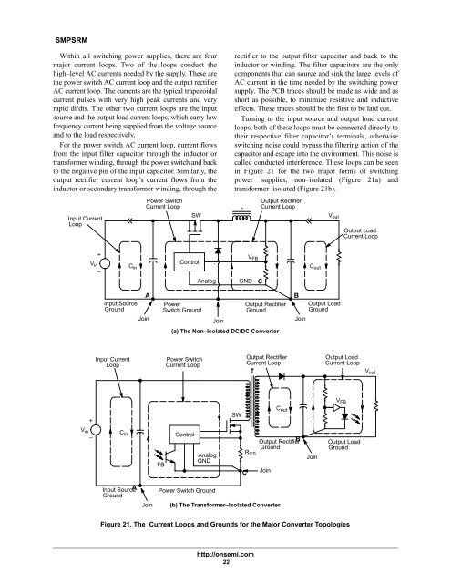
SMPSRMWithin all switching power supplies, there are fourmajor current loops. Two of the loops conduct thehigh–level AC currents needed by the supply. These arethe power switch AC current loop and the output rectifierAC current loop. The currents are the typical trapezoidalcurrent pulses with very high peak currents and veryrapid di/dts. The other two current loops are the inputsource and the output load current loops, which carry lowfrequency current being supplied from the voltage sourceand to the load respectively.For the power switch AC current loop, current flowsfrom the input filter capacitor through the inductor ortransformer winding, through the power switch and backto the negative pin of the input capacitor. Similarly, theoutput rectifier current loop’s current flows from theinductor or secondary transformer winding, through theInput CurrentLoop+V in–C in<strong>Power</strong> SwitchCurrent LoopSWControlAnalogrectifier to the output filter capacitor and back to theinductor or winding. The filter capacitors are the onlycomponents that can source and sink the large levels ofAC current in the time needed by the switching powersupply. The PCB traces should be made as wide and asshort as possible, to minimize resistive and inductiveeffects. These traces should be the first to be laid out.Turning to the input source and output load currentloops, both of these loops must be connected directly totheir respective filter capacitor’s terminals, otherwiseswitching noise could bypass the filtering action of thecapacitor and escape into the environment. This noise iscalled conducted interference. These loops can be seenin Figure 21 for the two major forms of switchingpower supplies, non–isolated (Figure 21a) andtransformer–isolated (Figure 21b).LGNDOutput RectifierCurrent LoopV FBCC outV outOutput LoadCurrent LoopInput SourceGroundAJoin<strong>Power</strong>Switch GroundJoinOutput RectifierGround(a) The Non–Isolated DC/DC ConverterBJoinOutput LoadGroundInput CurrentLoop<strong>Power</strong> SwitchCurrent LoopOutput RectifierCurrent LoopOutput LoadCurrent LoopV outV FB+SWC outV in–C inFBControlAnalogGNDCR CSOutput Rectifier BGroundJoinJoinOutput LoadGroundInput Source AGroundJoin<strong>Power</strong> Switch Ground(b) The Transformer–Isolated ConverterFigure 21. The Current Loops and Grounds for the Major Converter Topologieshttp://onsemi.com22