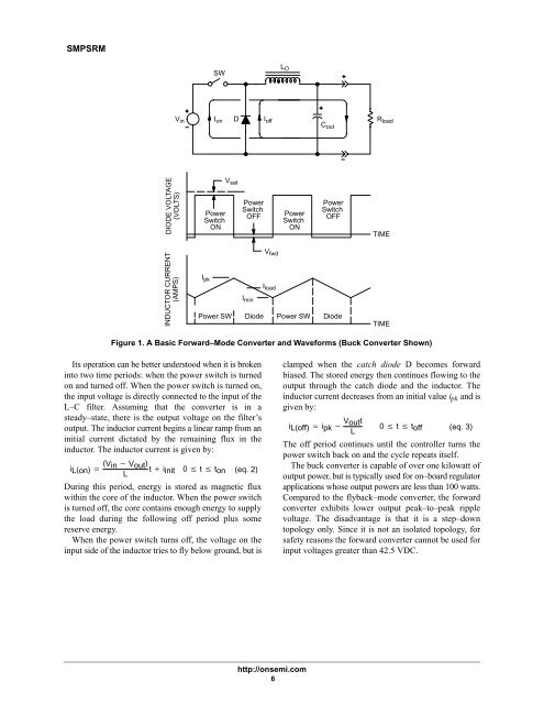
SMPSRMIntroductionThe never–ending drive towards smaller and lighterproducts poses severe challenges for the power supplydesigner. In particular, disposing of excess heatgenerated by power semiconductors is becoming moreand more difficult. Consequently it is important that thepower supply be as small and as efficient as possible, andover the years power supply engineers have responded tothese challenges by steadily reducing the size andimproving the efficiency of their designs.Switching power supplies offer not only higherefficiencies but also greater flexibility to the designer.Recent advances in semiconductor, magnetic and passivetechnologies make the switching power supply an evermore popular choice in the power conversion arena.This guide is designed to give the prospective designeran overview of the issues involved in designingswitchmode power supplies. It describes the basicoperation of the more popular topologies of switchingpower supplies, their relevant parameters, providescircuit design tips, and information on how to select themost appropriate semiconductor and passivecomponents. The guide also lists the ON Semiconductorcomponents expressly built for use in switching powersupplies.Linear versus Switching<strong>Power</strong> SuppliesSwitching and linear regulators use fundamentallydifferent techniques to produce a regulated outputvoltage from an unregulated input. Each technique hasadvantages and disadvantages, so the application willdetermine the most suitable choice.Linear power supplies can only step–down an inputvoltage to produce a lower output voltage. This is doneby operating a bipolar transistor or MOSFET pass unit inits linear operating mode; that is, the drive to the pass unitis proportionally changed to maintain the required outputvoltage. Operating in this mode means that there isalways a headroom voltage, Vdrop, between the inputand the output. Consequently the regulator dissipates aconsiderable amount of power, given by (Vdrop Iload).This headroom loss causes the linear regulator to onlybe 35 to 65 percent efficient. For example, if a 5.0 Vregulator has a 12 V input and is supplying 100 mA, itmust dissipate 700 mW in the regulator in order to deliver500 mW to the load , an efficiency of only 42 percent.The cost of the heatsink actually makes the linearregulator uneconomical above 10 watts for smallapplications. Below that point, however, linearregulators are cost–effective in step–down applications.A low drop–out (LDO) regulator uses an improvedoutput stage that can reduce Vdrop to considerably lessthan 1.0 V. This increases the efficiency and allows thelinear regulator to be used in higher power applications.Designing with a linear regulator is simple and cheap,requiring few external components. A linear design isconsiderably quieter than a switcher since there is nohigh–frequency switching noise.Switching power supplies operate by rapidly switchingthe pass units between two efficient operating states:cutoff, where there is a high voltage across the pass unitbut no current flow; and saturation, where there is a highcurrent through the pass unit but at a very small voltagedrop. Essentially, the semiconductor power switchcreates an AC voltage from the input DC voltage. ThisAC voltage can then be stepped–up or down bytransformers and then finally filtered back to DC at itsoutput. Switching power supplies are much moreefficient, ranging from 65 to 95 percent.The downside of a switching design is that it isconsiderably more complex. In addition, the outputvoltage contains switching noise, which must beremoved for many applications.Although there are clear differences between linearand switching regulators, many applications require bothtypes to be used. For example, a switching regulator mayprovide the initial regulation, then a linear regulator mayprovide post–regulation for a noise–sensitive part of thedesign, such as a sensor interface circuit.Switching <strong>Power</strong> <strong>Supply</strong>FundamentalsThere are two basic types of pulse–width modulated(PWM) switching power supplies, forward–mode andboost–mode. They differ in the way the magneticelements are operated. Each basic type has its advantagesand disadvantages.The Forward–Mode ConverterThe forward–mode converter can be recognized by thepresence of an L–C filter on its output. The L–C filtercreates a DC output voltage, which is essentially thevolt–time average of the L–C filter’s input ACrectangular waveform. This can be expressed as:Vout Vin duty cycle (eq. 1)The switching power supply controller varies the dutycycle of the input rectangular voltage waveform and thuscontrols the signal’s volt–time average.The buck or step–down converter is the simplestforward–mode converter, which is shown in Figure 1.http://onsemi.com5
SMPSRMSWL OV inI onDI offC outR loadDIODE VOLTAGE(VOLTS)<strong>Power</strong>SwitchONV sat<strong>Power</strong>SwitchOFF<strong>Power</strong>SwitchON<strong>Power</strong>SwitchOFFTIMEINDUCTOR CURRENT(AMPS)I pkI minV fwdI load<strong>Power</strong> SW Diode <strong>Power</strong> SW DiodeTIMEFigure 1. A Basic Forward–Mode Converter and Waveforms (Buck Converter Shown)Its operation can be better understood when it is brokeninto two time periods: when the power switch is turnedon and turned off. When the power switch is turned on,the input voltage is directly connected to the input of theL–C filter. Assuming that the converter is in asteady–state, there is the output voltage on the filter’soutput. The inductor current begins a linear ramp from aninitial current dictated by the remaining flux in theinductor. The inductor current is given by:iL(on) (V in Vout ) t Liinit 0 t ton (eq. 2)During this period, energy is stored as magnetic fluxwithin the core of the inductor. When the power switchis turned off, the core contains enough energy to supplythe load during the following off period plus somereserve energy.When the power switch turns off, the voltage on theinput side of the inductor tries to fly below ground, but isclamped when the catch diode D becomes forwardbiased. The stored energy then continues flowing to theoutput through the catch diode and the inductor. Theinductor current decreases from an initial value i pk and isgiven by:iL(off) ipk V outt0 t Ltoff (eq. 3)The off period continues until the controller turns thepower switch back on and the cycle repeats itself.The buck converter is capable of over one kilowatt ofoutput power, but is typically used for on–board regulatorapplications whose output powers are less than 100 watts.Compared to the flyback–mode converter, the forwardconverter exhibits lower output peak–to–peak ripplevoltage. The disadvantage is that it is a step–downtopology only. Since it is not an isolated topology, forsafety reasons the forward converter cannot be used forinput voltages greater than 42.5 VDC.http://onsemi.com6