SWITCHMODE⢠Power Supply Reference Manual
SWITCHMODE⢠Power Supply Reference Manual
SWITCHMODE⢠Power Supply Reference Manual

You also want an ePaper? Increase the reach of your titles
YUMPU automatically turns print PDFs into web optimized ePapers that Google loves.
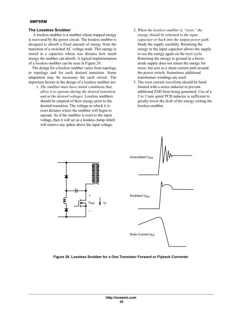
SMPSRMThe Lossless SnubberA lossless snubber is a snubber whose trapped energyis recovered by the power circuit. The lossless snubber isdesigned to absorb a fixed amount of energy from thetransition of a switched AC voltage node. This energy isstored in a capacitor whose size dictates how muchenergy the snubber can absorb. A typical implementationof a lossless snubber can be seen in Figure 29.The design for a lossless snubber varies from topologyto topology and for each desired transition. Someadaptation may be necessary for each circuit. Theimportant factors in the design of a lossless snubber are:1. The snubber must have initial conditions thatallow it to operate during the desired transitionand at the desired voltages. Lossless snubbersshould be emptied of their energy prior to thedesired transition. The voltage to which it isreset dictates where the snubber will begin tooperate. So if the snubber is reset to the inputvoltage, then it will act as a lossless clamp whichwill remove any spikes above the input voltage.2. When the lossless snubber is “reset,” theenergy should be returned to the inputcapacitor or back into the output power path.Study the supply carefully. Returning theenergy to the input capacitor allows the supplyto use the energy again on the next cycle.Returning the energy to ground in a boost–mode supply does not return the energy forreuse, but acts as a shunt current path aroundthe power switch. Sometimes additionaltransformer windings are used.3. The reset current waveform should be bandlimited with a series inductor to preventadditional EMI from being generated. Use of a2 to 3 turn spiral PCB inductor is sufficient togreatly lower the di/dt of the energy exiting thelossless snubber.Unsnubbed V SW+Snubbed V SWV SW I D–Drain Current (I D )Figure 29. Lossless Snubber for a One Transistor Forward or Flyback Converterhttp://onsemi.com28