Materials Science and Engineering Laboratory FY 2004 ... - NIST
Materials Science and Engineering Laboratory FY 2004 ... - NIST
Materials Science and Engineering Laboratory FY 2004 ... - NIST

Create successful ePaper yourself
Turn your PDF publications into a flip-book with our unique Google optimized e-Paper software.
<strong>Materials</strong> for Electronics<br />
Polymer Photoresists for Next-Generation Nanolithography<br />
Photolithography, the process used to fabricate<br />
integrated circuits, is the key enabler <strong>and</strong> driver<br />
for the microelectronics industry. As lithographic<br />
feature sizes decrease to the sub-100 nm length<br />
scale, significant challenges arise because both<br />
the image resolution <strong>and</strong> the thickness of the<br />
imaging layer approach the macromolecular<br />
dimensions characteristic of the polymers used<br />
in the photoresist film. Unique high-spatial<br />
resolution measurements are developed to<br />
reveal limits on materials <strong>and</strong> processes that<br />
challenge the development of photoresists for<br />
next-generation sub-100 nm lithography.<br />
Vivek M. Prabhu<br />
Photolithography is the driving technology used by<br />
the microelectronics industry to fabricate integrated<br />
circuits with ever decreasing sizes. In addition,<br />
this fabrication technology is rapidly being adopted<br />
in emerging areas such as optoelectronics <strong>and</strong><br />
biotechnology requiring the rapid creation of nanoscale<br />
structures. In this process, a designed pattern is<br />
transferred to the silicon substrate by altering the<br />
solubility of areas of a polymer-based photoresist<br />
thin film through an acid catalyzed deprotection<br />
reaction after exposure to radiation through a mask.<br />
To fabricate smaller features, next generation<br />
photolithography will be processed with shorter<br />
wavelengths of light requiring photoresist films<br />
less than 100 nm thick <strong>and</strong> dimensional control to<br />
within 2 nm.<br />
To advance this key fabrication technology, we<br />
work closely with industrial collaborators to develop<br />
<strong>and</strong> apply high-spatial resolution <strong>and</strong> chemically specific<br />
measurements to underst<strong>and</strong> changes in material<br />
properties, interfacial behavior, <strong>and</strong> process kinetics<br />
at nanometer scales that can significantly affect the<br />
patterning process.<br />
This year, we have continued to apply <strong>and</strong><br />
advance unique measurement methods to provide<br />
structural measurement of fabricated nanoscale<br />
structures <strong>and</strong> new insight <strong>and</strong> detail into the complex<br />
physico–chemical processes used in advanced<br />
chemically amplified photoresists. These methods<br />
include x-ray <strong>and</strong> neutron reflectivity (XR, NR), small<br />
angle x-ray <strong>and</strong> neutron scattering (SAXS, SANS),<br />
near-edge x-ray absorption fine structure spectroscopy<br />
(NEXAFS), combinatorial methods, solid state nuclear<br />
magnetic resonance (NMR), quartz crystal microbalance<br />
(QCM), fluorescence correlation spectroscopy (FCS),<br />
<strong>and</strong> atomic force microscopy (AFM).<br />
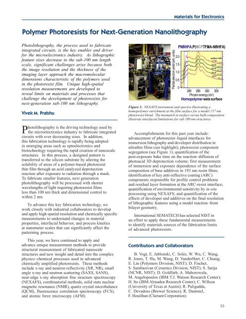
Figure 1: NEXAFS instrument <strong>and</strong> spectra illustrating a<br />
homopolymer enrichment at the film surface for a model 157 nm<br />
photoresist blend. The mismatch in surface versus bulk composition<br />
illustrate interfacial limitations for sub 100 nm structures.<br />
Accomplishments for this past year include:<br />
advancement of photoresist–liquid interfaces for<br />
immersion lithography <strong>and</strong> developer distribution in<br />
ultrathin films (see highlight); photoresist component<br />
segregation (see Figure 1); quantification of the<br />
post-exposure bake time on the reaction–diffusion of<br />
photoacid 3D deprotection volume; first measurement<br />
of immersion <strong>and</strong> exposure dependence of the surface<br />
composition of base additives in 193 nm resist films;<br />
identification of key anti-reflective coating (ARC)<br />
components responsible for profile control problems<br />
<strong>and</strong> residual layer formation at the ARC-resist interface;<br />
quantification of environmental sensitivity by in-situ<br />
processing using NEXAFS; <strong>and</strong> quantification of the<br />
effects of developer <strong>and</strong> additives on the final resolution<br />
of lithographic features using a model reaction–front<br />
bilayer geometry.<br />
International SEMATECH has selected <strong>NIST</strong> in<br />
an effort to apply these fundamental measurements<br />
to identify materials sources of the fabrication limits<br />
of advanced photoresists.<br />
Contributors <strong>and</strong> Collaborators<br />
B. Vogt, E. Jablonski, C. Soles, W. Wu, C. Wang,<br />
R. Jones, T. Hu, M. Wang, D. V<strong>and</strong>erHart, C. Chiang,<br />
E. Lin (Polymers Division, <strong>NIST</strong>); D. Fischer,<br />
S. Sambasivan (Ceramics Division, <strong>NIST</strong>); S. Satija<br />
(NCNR, <strong>NIST</strong>); D. Goldfarb, A. Mahorowala,<br />
M. Angelopoulos (IBM T.J. Watson Research Center);<br />
H. Ito (IBM Almaden Research Center); C. Willson<br />
(University of Texas at Austin); R. Puligadda,<br />
C. Devadoss (Brewer <strong>Science</strong>); R. Dammel,<br />
F. Houlihan (Clariant Corporation)<br />
35