Materials Science and Engineering Laboratory FY 2004 ... - NIST
Materials Science and Engineering Laboratory FY 2004 ... - NIST
Materials Science and Engineering Laboratory FY 2004 ... - NIST

Create successful ePaper yourself
Turn your PDF publications into a flip-book with our unique Google optimized e-Paper software.
<strong>Materials</strong> for Electronics<br />
Organic Electronics<br />
The field of organic electronics has dramatically<br />
emerged in recent years as an increasingly important<br />
technology encompassing a wide array of devices<br />
<strong>and</strong> applications including embedded passive<br />
devices, flexible displays, <strong>and</strong> sensors. Device<br />
performance, stability, <strong>and</strong> function critically<br />
depend upon charge transport <strong>and</strong> material<br />
interaction at the interfaces of disparate<br />
materials. We develop <strong>and</strong> apply non-destructive<br />
measurement methods to characterize the electronic<br />
<strong>and</strong> interfacial structure of organic electronics<br />
materials with respect to processing methods,<br />
processing variables, <strong>and</strong> materials characteristics.<br />
Eric K. Lin <strong>and</strong> Jan Obrzut<br />
Organic electronic devices are projected to<br />
revolutionize integrated circuits through new<br />
applications that take advantage of low-cost, highvolume<br />
manufacturing, nontraditional substrates, <strong>and</strong><br />
designed functionality. The current state of organic<br />
electronics is analogous to the early stages of the silicon<br />
electronics industry with the concurrent development<br />
of multiple material platforms <strong>and</strong> processes, <strong>and</strong> a lack<br />
of measurement st<strong>and</strong>ardization between laboratories.<br />
A critical need exists for new diagnostic probes, tools,<br />
<strong>and</strong> methods to address new technological challenges.<br />
Organic electronics presents fundamentally<br />
different measurement challenges from those identified<br />
for inorganic devices. The adoption of this technology<br />
will be advanced by the development of an integrated<br />
suite of metrologies to correlate device performance<br />
with the structure, properties, <strong>and</strong> chemistry of<br />
materials <strong>and</strong> interfaces. We are developing<br />
measurement methods to provide the data <strong>and</strong> insight<br />
needed for the rational <strong>and</strong> directed development<br />
of emerging materials <strong>and</strong> processes.<br />
This year, we have addressed three areas covering<br />
a spectrum of active organic electronic materials:<br />
dielectric measurements for embedded passive devices,<br />
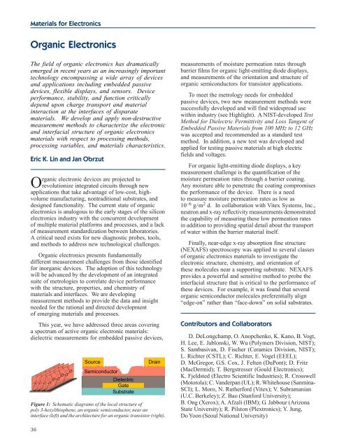
Figure 1: Schematic diagrams of the local structure of<br />
poly 3-hexylthiophene, an organic semiconductor, near an<br />
interface (left) <strong>and</strong> the architecture for an organic transistor (right).<br />
36<br />
measurements of moisture permeation rates through<br />
barrier films for organic light-emitting diode displays,<br />
<strong>and</strong> measurements of the orientation <strong>and</strong> structure of<br />
organic semiconductors for transistor applications.<br />
To meet the metrology needs for embedded<br />
passive devices, two new measurement methods were<br />
successfully developed <strong>and</strong> will find widespread use<br />
within industry (see Highlight). A <strong>NIST</strong>-developed Test<br />
Method for Dielectric Permittivity <strong>and</strong> Loss Tangent of<br />
Embedded Passive <strong>Materials</strong> from 100 MHz to 12 GHz<br />
was accepted <strong>and</strong> recommended as a st<strong>and</strong>ard test<br />
method. In addition, a new test was developed <strong>and</strong><br />
applied for testing passive materials at high electric<br />
fields <strong>and</strong> voltages.<br />
For organic light-emitting diode displays, a key<br />
measurement challenge is the quantification of the<br />
moisture permeation rates through a barrier coating.<br />
Any moisture able to penetrate the coating compromises<br />
the performance of the device. There is a need<br />
to measure moisture permeation rates as low as<br />
10 –6 g/m 2 d. In collaboration with Vitex Systems, Inc.,<br />
neutron <strong>and</strong> x-ray reflectivity measurements demonstrated<br />
the capability of measuring these low permeation rates<br />
in addition to providing spatial detail about the transport<br />
of water within the barrier material itself.<br />
Finally, near-edge x-ray absorption fine structure<br />
(NEXAFS) spectroscopy was applied to several classes<br />
of organic electronics materials to investigate the<br />
electronic structure, chemistry, <strong>and</strong> orientation of<br />
these molecules near a supporting substrate. NEXAFS<br />
provides a powerful <strong>and</strong> sensitive method to probe the<br />
interfacial structure that is critical to the performance of<br />
these devices. For example, it was found that several<br />
organic semiconductor molecules preferentially align<br />
“edge-on” rather than “face-down” on solid substrates.<br />
Contributors <strong>and</strong> Collaborators<br />
D. DeLongchamp, O. Anopchenko, K. Kano, B. Vogt,<br />
H. Lee, E. Jablonski, W. Wu (Polymers Division, <strong>NIST</strong>);<br />
S. Sambasivan, D. Fischer (Ceramics Division, <strong>NIST</strong>);<br />
L. Richter (CSTL); C. Richter, E. Vogel (EEEL);<br />
D. McGregor, G.S. Cox, J. Felten (DuPont); D. Fritz<br />
(MacDermid); T. Bergstresser (Gould Electronics);<br />
K. Fjeldsted (Electro Scientific Industries); R. Crosswell<br />
(Motorola); C. V<strong>and</strong>erpan (UL); R. Whitehouse (Sanmina-<br />
SCI); L. Moro, N. Rutherford (Vitex); V. Subramanian<br />
(U.C. Berkeley); Z. Bao (Stanford University);<br />
B. Ong (Xerox); A. Afzali (IBM); G. Jabbour (Arizona<br />
State University); R. Pilston (Plextronics); Y. Jung,<br />
Do Yoon (Seoul National University)